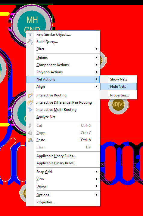
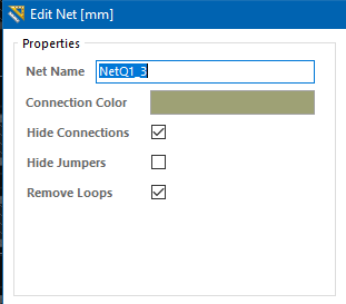
When you first start to place your components on the PCB all of the rat nest lines are total chaos.
When I use Eagle I like to hide selected rat nest lines (namely VCC and GND) as these will generally connect to an internal power plane or polygon pour. This de-clutters the rat nest lines and allows me to then focus on the general inter-component connections.
How do I hide selected rat nest lines in Altium PCB?
Note: This question is similar to this one but I only want to hide selected rat nest lines, not all of them.


