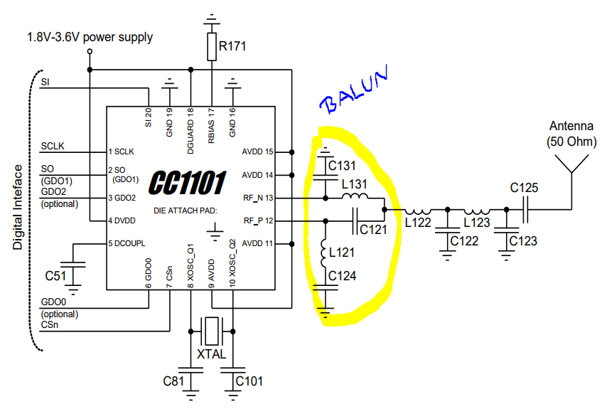
According to the data sheet, \$\small C_{124}\$ is a relatively high value decoupling capacitor and \$\small L_{131}C_{131}= L_{121}C_{121}=LC =1/{{\omega_{n}}^2}\$. Component values are: \$\small L=33nH;\:C=6.8pF\$, giving a natural frequency of \$\small\omega_n=2.11\times 10^9 rad/sec\$, or \$\small f_n= 336MHz\$, which will lead to a slightly lower resonant frequency, \$\small f_r\$, in a practical circuit where resistance is taken into account.
Assume now some small series resistance, \$\small R\$, in each of the branches leading to pins 12 and 13, hence we have two series L/C/R circuits with the \$\small V_n\$ and \$\small V_p\$ signals taken across the capacitor and inductor respectively. Using the voltage divider rule, \$\small V_n\$ and \$\small V_p\$ may be expressed in terms of the input voltage to the balun, \$\small V_i\$ (i.e. the signal at the junction of \$\small L_{122}/L_{131}/C_{121}\$) as:
$$\small V_n=\frac{\frac{1}{LC}}{s^2+\frac{R}{L}s+\frac{1}{LC}}V_i $$
$$\small V_p=\frac{s^s}{s^2+\frac{R}{L}s+\frac{1}{LC}}V_i$$
Writing these in standard form:
$$\small V_n=\frac{\omega_n^2}{s^2+2\zeta\omega_n s+\omega_n^2}V_i $$
$$\small V_p=\frac{s^2}{s^2+2\zeta\omega_n s+\omega_n^2}V_i$$
where \$\small \zeta=\frac{R}{2}\sqrt{\frac{C}{L}}\$
Notice that \$\small V_n\$ and \$\small V_p \$ are low-pass and high-pass filtered versions of \$\small V_i \$, respectively.
Moving now from Laplace domain to frequency domain (\$\small s\rightarrow j\omega \$):
$$\small V_n=\frac{\omega_n^2}{(\omega_n^2-\omega^2)+j2\zeta\omega\omega_n}V_i $$
$$\small V_p=\frac{-\omega^2}{(\omega_n^2-\omega^2)+j2\zeta\omega\omega_n}V_i$$
Now let \$\small \omega=\omega_n\$:
$$\small V_n=\frac{\omega_n^2}{j\:2\zeta \omega_n^2}V_i\:=\:\frac{-j}{2\zeta}V_i =\frac{V_i}{2\zeta}\large\angle\small-90^o$$
$$\small V_p=\frac{-\omega_n^2}{j\:2\zeta \omega_n^2}V_i\:=\:\frac{j}{2\zeta}V_i =\frac{V_i}{2\zeta}\large\angle\small+90^o $$
Hence \$\small V_p\$ and \$\small V_n\$ are the same magnitude but phase shifted by \$\small 180^o\$, i.e. one is the inverse on the other, so when they are subtracted:
$$\small V_p-V_n=\frac{V_i}{\zeta}\large\angle\small+90^o$$
Using the values for \$\small L\$ and \$\small C\$ given in the data sheet, \$\small \zeta =7.2\times 10^{-3}R\$, and the voltage gain at \$\small 336 \:MHz\$ will be large (around \$\small 60\:dB\$ for \$\small R=0.1\Omega\$). This gain reduces to around \$\small 15\:dB\$ at the operational frequency of \$\small 315 \:MHz\$.
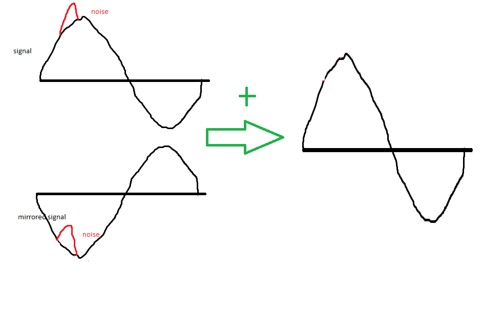
Common mode noise signals are rejected due to the subtraction performed on the \$\small V_p\$ and \$\small V_n\$ signals.
 I am trying to understand the balun of the CC1101 circuit :
 .
As I understand it, the balun is usefull to reject common mode noise picked up by the RF cable.