3
\$\begingroup\$

I'm trying to build a circuit that realizes the transfer function: $$ V_o = 0.33V_i + 1.65V $$

Using what I know about voltage dividers and resistive adders, I built:

schematic

simulate this circuit – Schematic created using CircuitLab

but this is giving me an output much closer to: $$V_o = 0.2V_i + 1V$$

Where am I going wrong?

\$\endgroup\$
9
  • \$\begingroup\$ I would rather think about an amplifier circuit than a resistors nework.. \$\endgroup\$
    – Eugene Sh.
    Commented Jan 19, 2018 at 17:10
  • \$\begingroup\$ Is this just a homework problem or are you actually trying to use this for a real-world problem? If the latter it sounds like an XY problem and you should describe your problem rather than your approach. \$\endgroup\$
    – loudnoises
    Commented Jan 19, 2018 at 17:16
  • 1
    \$\begingroup\$ @loudnoises It's actually for a real-world problem. I need to scale V_i from a range of (-5, +5)V to a range of (0, 3.3)V \$\endgroup\$
    – janizer
    Commented Jan 19, 2018 at 17:18
  • 2
    \$\begingroup\$ You can't really do a summer using passive components. This is because there is nothing to isolate the sides from each other. What your actually getting is more of an averager. The voltage divider on each side affects the voltage divider of the other side. Further, the destination of the voltage needs to be of a very high input impedance because then the destination will also affect the reading. This should really be done using opAmps. \$\endgroup\$
    – vini_i
    Commented Jan 19, 2018 at 17:34
  • 1
    \$\begingroup\$ There are two things to consider. The mcu input is slightly capacitive and with an AC signal this will cause some amount of loading. Also the ADC will be a sample and hold. This means it will need to charge a capacitor. The output impedance will limit how fast that capacitor will charge limiting the sampling rate. \$\endgroup\$
    – vini_i
    Commented Jan 21, 2018 at 19:03

5 Answers 5

8
\$\begingroup\$

There are two problems with your design.

  1. A voltage divider only produces it's notional output voltage when unloaded.
  2. Your second stage forms an averaging circuit not a sum.

Bottom line is that your approach isn't going to be fruitful.


Fortunately a much simpler design will solve your problem. We just need a weighted average circuit.

For ease of calculation i'm going to assume that when you wrote 0.33 you meant \$\frac{1}{3}\$ if you want to actually use 0.33 that makes the numerics less nice but does'nt change the principles.

We can rewrite your equation as a weighted average and implement it as a weighted average circuit. This consists of three resistors, one from the input to the output, one from 3.3V to the output and one from ground to the output.

$$V_o = \frac{1}{3}V_i + 1.65 = \frac{2}{6}V_i + \frac{3}{6}3.3+\frac{1}{6}0$$

(note that our weights add up to 1 and all of them are positive, that is important)

Now we simply take the reciprocal of the weights to work out our resistor values.

$$R_{Vi} = \frac{6}{2}R$$ $$R_{3.3V} = \frac{6}{3}R$$ $$R_{Ground} = \frac{6}{1}R$$

Where \$R\$ is the output impedance of our weighted average circuit.

Then it becomes a matter of picking a \$R\$ value to set the actual value of our resistors. Ideally we want to pick it such that all three values are standard values. Turns out that \$R=0.5\mathrm{k}\Omega\$ works out nicely giving us.

$$R_{Vi} = \frac{6}{2}R = 1.5\mathrm{k}\Omega$$ $$R_{3.3V} = \frac{6}{3}R = 1\mathrm{k}\Omega$$ $$R_{Ground} = \frac{6}{1}R = 3\mathrm{k}\Omega$$

\$\endgroup\$
1
  • \$\begingroup\$ Works great. Thanks for walking me through your reasoning! \$\endgroup\$
    – janizer
    Commented Jan 21, 2018 at 16:08
5
\$\begingroup\$

Here's an answer:

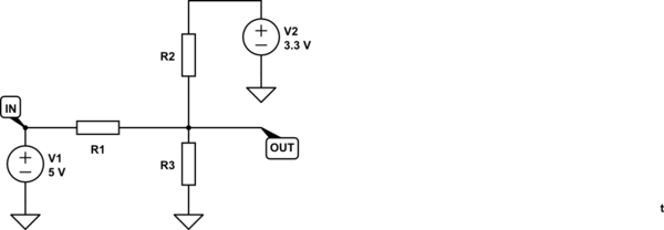
schematic

simulate this circuit – Schematic created using CircuitLab

Figure 1. The complete circuit.

Here's how to work it out:

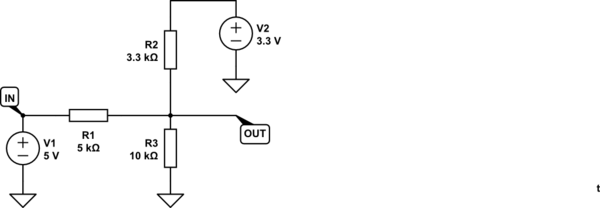
We're going to need a divider to zero volts to pull the high voltage down and a resistor to +3.3 V to pull the -5 V up. That gives us the circuit layout of Figure 1. Next we need to work out the component values.

Calculating R2

schematic

simulate this circuit

Figure 2. At -5 V input.

  • At -5 V in you want 0 V on the output. Therefore R3 is doing nothing (since both ends are at 0 V). Let's leave it out for a moment.
  • Now select R1 and R2 in the ratio of 5 to 3.3. 5k and 3k3 are an obvious choice. Now with IN = -5 V, OUT = 0 V.

Calculating R3

schematic

simulate this circuit

Figure 3. At +5 V in we get +3.3 V out.

  • At +5 V in we want 3.3 V out.
  • Since both ends of R2 will be at 3.3 V we can leave it out for the moment.
  • Now we just need to divide down by 1/3 to convert +5 V to +3.3 V.
  • Since R1 is already determined as 5k then R3 must be twice that, so 10k. Now with IN = +5 V, OUT = 3.3 V.

The result

schematic

simulate this circuit

Checking the result

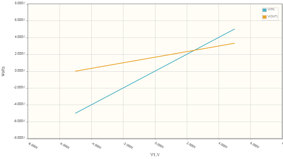
enter image description here

Figure 4. The result of a simulated sweep from -5 to +5 V on the input.

It's what you want.

\$\endgroup\$
3
\$\begingroup\$

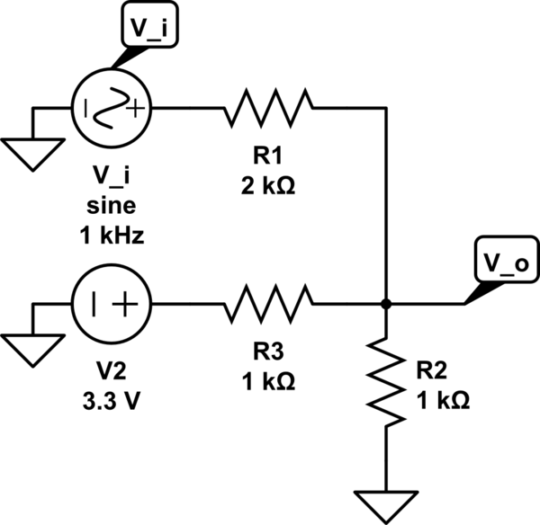
The circuit can be simplified down to 3 resistors. Calculating the value of those resistors requires either iteration or the use of simultaneous equations.

schematic

simulate this circuit – Schematic created using CircuitLab

1) Pick an output resistor value (R2). Choose an initial value of resistor value for R3.

2) Replace the DC voltage source with a short circuit. Calculate the value of R1 to give you the desired attenuation at V_o.

3) Replace the AC voltage source with a short circuit. Given the values already chosen for R1 & R2, change the value of R3 to give you the desired offset voltage.

Iterate the values of R1 & R3 until both the AC signal attenuation and the DC offset are correct.

Alternatively, create two equations that describe the output: one equation is for when the DC source is shorted; the other equation is for when the AC source is shorted. Simple algebra will allow you to solve for the values of R1 & R3.

The reason that I mention iteration first when solving this problem is that I use a math package called "TK Solver". I simply write two equations (as described above) and feed them into TK Solver. This software package uses iteration to converge on the desired resistor values. Very, very quick.

\$\endgroup\$
3
\$\begingroup\$

You only need three resistors to produce your transfer function.

schematic

simulate this circuit – Schematic created using CircuitLab

The equation for the circuit is... $$ V_{out} = \frac { \frac {V_{in}}{R1} + \frac {V_{CC}}{R2} } { \frac {1}{R1} + \frac {1}{R2} + \frac {1}{R3} } \tag {EQ1} $$

You want to produce a transfer function that looks like...

$$ V_{out} = 0.33 V_{in} + 1.65 \tag {EQ2} $$

Equating EQ1 and EQ2 gives...

$$ V_{out} = \frac { \frac {V_{in}}{R1} + \frac {V_{CC}}{R2} } { \frac {1}{R1} + \frac {1}{R2} + \frac {1}{R3} } = 0.33 V_{in} + 1.65 $$ Both equations contain a constant term and a term that is proportional to Vin. Therefore we can separate them into two equations (one for the proportional term and the other for the constant term) ...

$$ \frac { \frac {V_{in}}{R1} }{ \frac {1}{R1} + \frac {1}{R2} + \frac {1}{R3} } = 0.33 V_{in} \tag {EQ3} $$
$$ \frac {\frac {V_{CC}}{R2}} { \frac {1}{R1} + \frac {1}{R2} + \frac {1}{R3} } = 1.65 \tag {EQ4} $$

We now have two equations and three unknowns.

Dividing EQ3 by EQ4 and solving for R2 gives us... $$ R2 = R1 \cdot 0.33 \cdot \frac {V_{CC}} {1.65} \tag {EQ5} $$

Plugging in EQ5 into EQ3 and solving for R3 gives... $$ R3 = \frac {0.33 \cdot R1}{1 - 0.33 - \frac {1.65}{V_{CC}} } \tag {EQ6} $$

We have three resistors, but because EQ3 and EQ4 only created two constraints the system is under-constrained. This means we may arbitrarily pick one of the resistors. Because of the structure of EQ5 and EQ6 it is probably easiest to pick R1.

For example, if we pick R1 = 1 kΩ and VCC = 3.3 V we get... $$ R2 = \frac {1 \mathrm {k\Omega} \cdot 0.33 \cdot 3.3 \mathrm V} {1.65 \mathrm V} = 0.66 \mathrm {k\Omega} $$

$$ R3 = \frac {0.33 \cdot 1\ \mathrm {k\Omega}} {1 - 0.33 - \frac {1.65\ \mathrm V}{3.3\ \mathrm V}} = 1.941\ \mathrm {kΩ} $$

\$\endgroup\$
1
  • \$\begingroup\$ I've MathJAXed the equations for you but left the originals to simplify proof reading. Delete either as you please. \$\endgroup\$
    – Transistor
    Commented Jan 20, 2018 at 6:58
2
\$\begingroup\$

You are trying to map ±5 V to 0-3.3 V. Try something like this:

schematic

simulate this circuit – Schematic created using CircuitLab

The first section reduces the voltage down to around ±1.15 V. The capacitor prevents DC from travelling between sections. The second resistor divider biases the signal around 1.65 V. This will work well if you are not driving much of a load, but if you are then put an op-amp buffer after it. Make sure that the capacitor is big enough that it doesn't filter any of your wanted signal.

\$\endgroup\$
2
  • 1
    \$\begingroup\$ OP didn't say the signal was AC. It might vary between -5 and +5 V in a week. \$\endgroup\$
    – Transistor
    Commented Jan 19, 2018 at 19:28
  • 1
    \$\begingroup\$ That’s true, however it is unspecified and this answer would work for a broad subset of problems. \$\endgroup\$
    – loudnoises
    Commented Jan 19, 2018 at 21:25

Your Answer

By clicking “Post Your Answer”, you agree to our terms of service and acknowledge you have read our privacy policy.

Not the answer you're looking for? Browse other questions tagged or ask your own question.