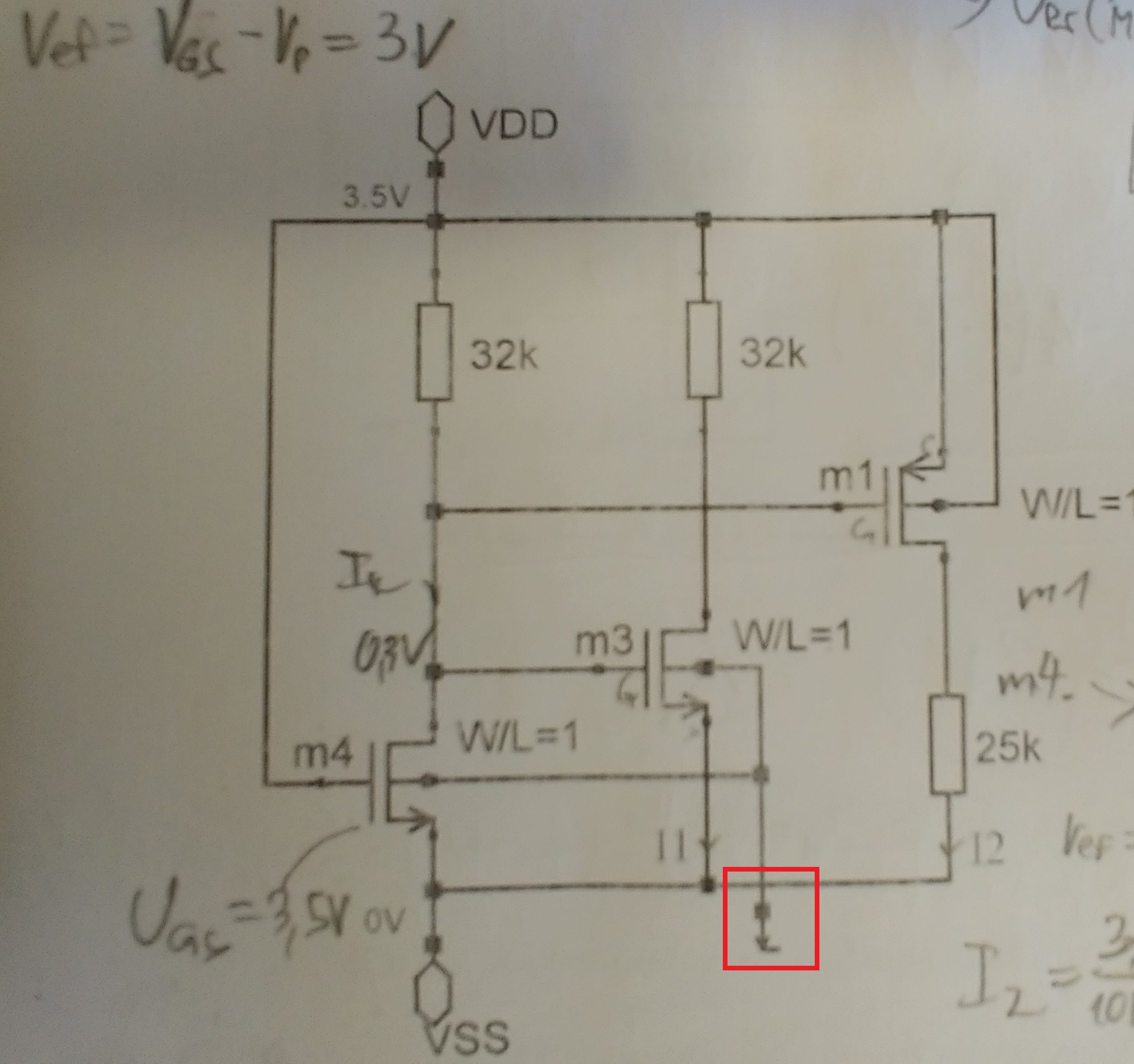
I found a circuit diagram, which I do not understand. In the diagram below, I bounded a peculiar terminal with a red box. The bulk of m3 and m4 MOSFETs are connected to this negative terminal.
My question is, what does this mean? Does this mean that the bulk of m4 and m3 is connected to some terminal that has a potential lower than VSS?
I appreciate any help.

