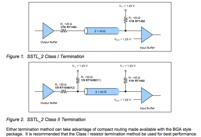
added: Which bus termination scheme did you use?
 method (1) is preferred, Is 1.25Vdc clean?
Did pay for ICT on these boards? bare board test is a must
Did you specify impedance on your gerber layout instructions?
Did you run simulations on your layout with tolerances?
Dielectric constant on boards and #of layers of pre-preg control the impedance of stripline and microstrip along with trace width and gap.
There are many free online Z calculators for stripline.
You can try to measure capacitance on large tracks or ground planes and compare both bare boards.
Also look at the signals with a high speed scope and observe overshoot and clock<>data eye pattern.
There has to be a simple explanation for the errors, but its not easy to find. But once you find the root cause... you won't make that mistake again.
added: Another mistake I found is your stack height diagram does not indicate the Cu layer thickness and there is insufficient to fit in 6 layers unless it is wrong or the Cu thickness is 0.039 mm (NOT ;)
