2nd add We assumed your design was margin tested and the code was perfect in your questions. (not) I suggest you verify the following;
- Configure the IO to have fast slew and disable the input filters
- Enable the input mode on the clock
- Set the slew bit (9?) to increase the slew rate for the SDRAM interface pins
- Enable repeater mode since they are bi-directional and must not be left floating on a cmos input.
- Change the supply voltage to determine sensitivity to error.
- default reset mode for a data bus pin is FUNC=0X00, MODE=0X02, HYSTERESIS=ENABLED, INVERT=DISABLED, and SLEW=STANDARD
- Does your call to PINSEL_ConfigPin() with a new function value, reset the MODE to INACTIVE (no pull-down/pull-up resistor) and turn off HYSTERESIS?
- Are you using a for/next loops or discrete code such as;
- LPC_IOCON->P3_0 |= 1; // D0 @ P3.0
- LPC_IOCON->P3_1 |= 1; // D1 @ P3.1
- LPC_IOCON->P3_2 |= 1; // D2 @ P3.2 etc.
- Do you assert to re-enable the WE pin, every time when needed?
- Do you use? *pPIN &= ~(0x00000007);//Clear function bits"
I remember debugging my 1st CMOS design from a Physics post grad student for a Seismic portable recording, switchable timer logic board. There was no firmware or uC but he never did a worst case tolerance analysis and the hardware had race conditions all over the place when a dozen more boards were built and debugged by myself. The Seismic Prof brought over the Head of Physics Dept to ask why I could not make debug the boards, then I had to advise him component variation exposed many design flaws called timing race conditions due to metastable conditions and clock edge used. He still still didn't understand, then I asked him tell me how many fingers I unfolded while I was raising my hand before it reached my waist level from low to high. Then he said , you can't do that and expect a correct answer. I said, precisely. Thats a primitive race condition. They get less obvious with more levels of complexity. U of Manitoba 1973.
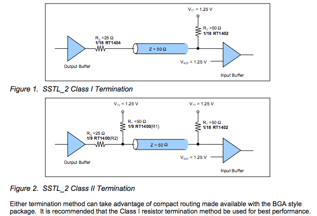
1st added: Which bus termination scheme did you use?
 method (1) is preferred, Is 1.25Vdc clean?
Did pay for ICT on these boards? bare board test is a must
Did you specify impedance on your gerber layout instructions?
Did you run simulations on your layout with tolerances?
Dielectric constant on boards and #of layers of pre-preg control the impedance of stripline and microstrip along with trace width and gap.
There are many free online Z calculators for stripline.
You can try to measure capacitance on large tracks or ground planes and compare both bare boards.
Also look at the signals with a high speed scope and observe overshoot and clock<>data eye pattern.
There has to be a simple explanation for the errors, but its not easy to find. But once you find the root cause... you won't make that mistake again.
added: Another mistake I found is your stack height diagram does not indicate the Cu layer thickness and there is insufficient to fit in 6 layers unless it is wrong or the Cu thickness is 0.039 mm (NOT ;)
