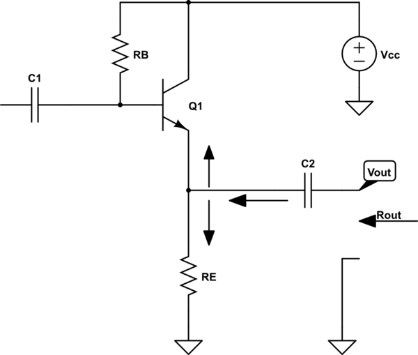
The simplest common collector amplifier looks like this:

simulate this circuit – Schematic created using CircuitLab
And now if we are looking form the load resistance perspective. We see two paths for a current to flow.
One path is through the \$R_E\$ resistor into GND.
And the second path is into the transistor emitter terminal.
And this is why the load is seeing two "resistances" in parallel.
\$R_{OUT} = R_E||(r_e + \frac{R_B}{\beta+1})\$
Or you can see it this way. The NPN transistor can only "source" the current into the load resistance. And \$R_E\$ resistor can "sink" the load current.
