Answer
Part A - Operation described
If the push button S1 is pressed, LED1 will turn on; if push button is released, LED1 will turn off.
Part B - Operation explained
(1) When S1 is pressed, current flows through photo diode U1.
(2) U1 is a actually a LED (Light Emitted Diode), so light (photons) will be emitted and hit the Base of the the photo transistor.
(3) The photons hitting the Base will be absorbed by the Base, and positive charge carriers (more precisely "holes") will be created at the Base and as more and more charge carriers (holes) build up at the Base, a voltage potential is formed between the Base and Ground, causing a current flow from Base to Ground. Let us call this current Ib, which incidentally is small, because U1 is a weak guy, and cannot create too many photons to cause big enough current to wake up its neighbour, the photo transistor.
(4) Luckily the transistor is a clever guy. It is basically a current amplifier, amplifying the small Base current to a big current flowing from Collect to Emitter. Let us call this amplified current Ic.
(5) Now of course Ic flows through LED1 as well.
(6) What will LED1 will now do then? Ah, it is time for me to prepare my locking down supper. Perhaps the OP can complete the story and write up his lab report, including an acknowledgement to the EE SE perhaps? :)
References
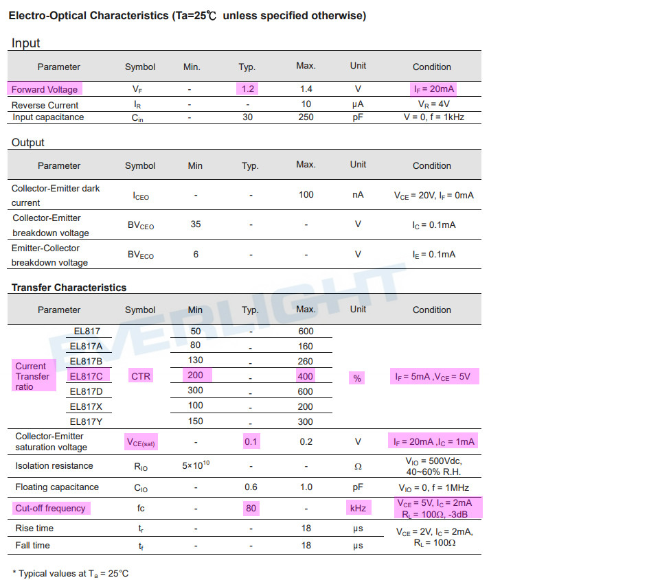
EL817 PhotoTransistor OctoCoupler Datasheet - EverBright
Appendices
Appendix A - Photo Transistor
Photodiode - Wikipedia
A photodiode is a semiconductor device that converts light into an electrical current. The current is generated when photons are absorbed in the photodiode.
Photodiodes may contain optical filters, built-in lenses, and may have large or small surface areas.
Photodiodes usually have a slower response time as their surface area increases. The common, traditional solar cell used to generate electric solar power is a large area photodiode.
Photodiodes are similar to regular semiconductor diodes except that they may be either exposed (to detect vacuum UV or X-rays) or packaged with a window or optical fiber connection to allow light to reach the sensitive part of the device. Many diodes designed for use specially as a photodiode use a PIN junction rather than a p–n junction, to increase the speed of response. A photodiode is designed to operate in reverse bias.
...
Related devices - Phototransistor
...
A phototransistor is a light-sensitive transistor. A common type of phototransistor, the bipolar phototransistor, is in essence a bipolar transistor encased in a transparent case so that light can reach the base–collector junction.
It was invented by Dr. John N. Shive (more famous for his wave machine) at Bell Labs in 1948 but it was not announced until 1950. The electrons that are generated by photons in the base–collector junction are injected into the base, and this photodiode current is amplified by the transistor's current gain β (or hfe).
If the base and collector leads are used and the emitter is left unconnected, the phototransistor becomes a photodiode. While phototransistors have a higher responsivity for light they are not able to detect low levels of light any better than photodiodes.
Phototransistors also have significantly longer response times. Another type of phototransistor, the field-effect phototransistor (also known as photoFET), is a light-sensitive field-effect transistor. Unlike photobipolar transistors, photoFETs control drain-source current by creating a gate voltage.
A solaristor is a two-terminal gate-less phototransistor. A compact class of two-terminal phototransistors or solaristors have been demonstrated in 2018 by ICN2 researchers.
The novel concept is a two-in-one power source plus transistor device that runs on solar energy by exploiting a memresistive effect in the flow of photogenerated carriers.
Appendix B - Optocoupler EL817C Datasheet

