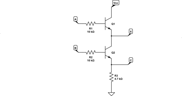
I'll focus on the poor AND circuit:

simulate this circuit – Schematic created using CircuitLab
There are four conditions, as you've suggested. Take each one in turn, given your statement about \$V_{_\text{CC}}=6\:\text{V}\$ and nominally for initial analysis purposes, \$LO=0\:\text{V}\$ and \$HI=6\:\text{V}\$. (In all cases, while we may not know the exact value for \$X\$, we do know that it cannot be below ground nor above \$V_{_\text{CC}}\$.)
Before I continue, there is a BJT parameter you can find on datasheets: \$I_{_\text{CBO}}\$. This is the collector cutoff current. For example, from this old datasheet on the 2N2222 you can see the value at room temperature and with \$50\:\text{V}\$ of reverse CB voltage, \$I_{_\text{CBO}}\le 10\:\text{nA}\$ and at \$150^\circ\:\text{C}\$ it rises to \$I_{_\text{CBO}}\le 10\:\mu\text{A}\$ (1000 times higher.) Either way, these are very tiny currents. For below, let's just assume \$I_{_\text{CBO}}= 50\:\text{nA}\$. (In practice and in Spice it will not be that high.)
- \$A=LO\$ and \$B=LO\$: \$Q_1\$ is off, regardless of \$X\$, and therefore the collector/base junction is reverse-biased by about \$6\:\text{V}\$ and we can assume only a small \$I_{_\text{CBO}}\$ via \$R_1\$, meaning the base voltage will be about \$500\:\mu\text{V}\$. We don't know how the emitter current, yet. So we can't estimate the emitter voltage. But it should be near this value, perhaps tugged only slightly upward by its disconnected collector voltage (if \$Q_2\$ is off) and otherwise tugged down by \$Q_2\$'s collector. Ah. But \$Q_2\$ is off, too. \$X\$ is pretty much floating. This suggests almost no \$Q_1\$ emitter current -- call it zero because that's about what it is. So there's no real voltage at \$Q_2\$'s collector. It's just floating. So not even \$I_{_\text{CBO}}\$ in \$Q_2\$. So \$Q_2\$'s base is hugged tight to ground and should be very close to it. As there is no emitter current in \$Q_1\$ there cannot be any emitter current in \$Q_2\$, either. So \$R_3\$ pulls the output down almost exactly to ground. Output impedance is \$R_3\$.
- \$A=HI\$ and \$B=LO\$: \$Q_1\$ is active. But \$Q_2\$ is off. so we expect at most \$I_{_\text{CBO}}\$ in \$Q_2\$. That current has to come from \$Q_1\$'s emitter. But as only \$\frac1{\beta+1}\$ of it comes via \$R_1\$, we can pretty much say the base of \$Q_1\$ is also at \$6\:\text{V}\$. It's emitter will be about \$V_T\cdot\ln\left(\frac{I_{_\text{CBO}}}{I_{_\text{SAT}}}\right)\$ or perhaps as much as a few hundred millivolts across the BE junction of \$Q_1\$. So we'd expect \$Q_2\$'s collector to be within a few hundred millivolts of \$V_{_\text{CC}}\$. That still doesn't mean there's any emitter current in \$Q_2\$, though. So, again, \$R_3\$ pulls the output down almost exactly to ground. Output impedance is \$R_3\$.
- \$A=LO\$ and \$B=HI\$: \$Q_1\$ is off. So its emitter current is basically zero. But \$Q_2\$ is active, now. While there's no \$Q_2\$ collector current to speak of, you do have two resistors present. So the emitter current is \$\frac{V_{_\text{CC}}-V_{_\text{BE}}}{R_3+R_2}\$ and, after multiplying that current by \$R_3\$, gives about \$1.7\:\text{V}\$ at the output. This is not really \$LO\$ nor is it really \$HI\$. So this is probably a bad AND gate. Output impedance is about \$R_3\mid\mid R_2\$.
- \$A=HI\$ and \$B=HI\$: Both \$Q_1\$ and \$Q_2\$ are now active and now there can be some emitter current from \$Q_1\$ into \$Q_2\$'s collector. So in this case, the emitter current of \$Q_2\$ is \$\frac{V_{_\text{CC}}-V_{_\text{BE}}}{R_3+\frac{R_2}{\beta+1}}\$ and, after multiplying that current by \$R_3\$, gives about \$5.2\:\text{V}\$ at the output. Again, this isn't exactly \$LO\$ nor is it really \$HI\$. But it's perhaps close enough to \$HI\$ to be tolerable. Output impedance is closer now to \$\frac{R_2}{\beta+1}\$, which is almost low enough to be useful.
In short, I'd say that this isn't really a good AND gate.
