The “default” LTspice transistor is idealized. Real ones aren’t that good :)
Bipolar transistors are called “switches” but they are not literal switches like a toggle switch is – they are not mechanical contacts.
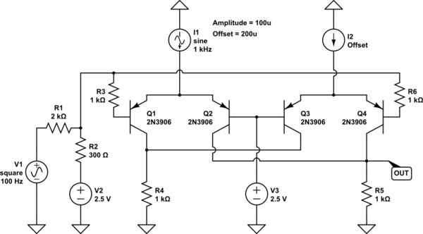
Perhaps inadvertently, you have set up the transistor as a common-base switch, and that has a chance of working acceptably – you just need some load, the output can’t float.
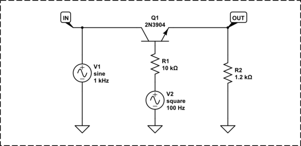
simulate this circuit – Schematic created using CircuitLab
The component values do depend on the parameters of the transistor, and have to be adjusted in practice. It's not the best way to implement a switch, but it certainly works well enough to be useful for something.
The general idea for common-base switches is having ample amplitude of base drive. Ideally, the base drive would be a current source.
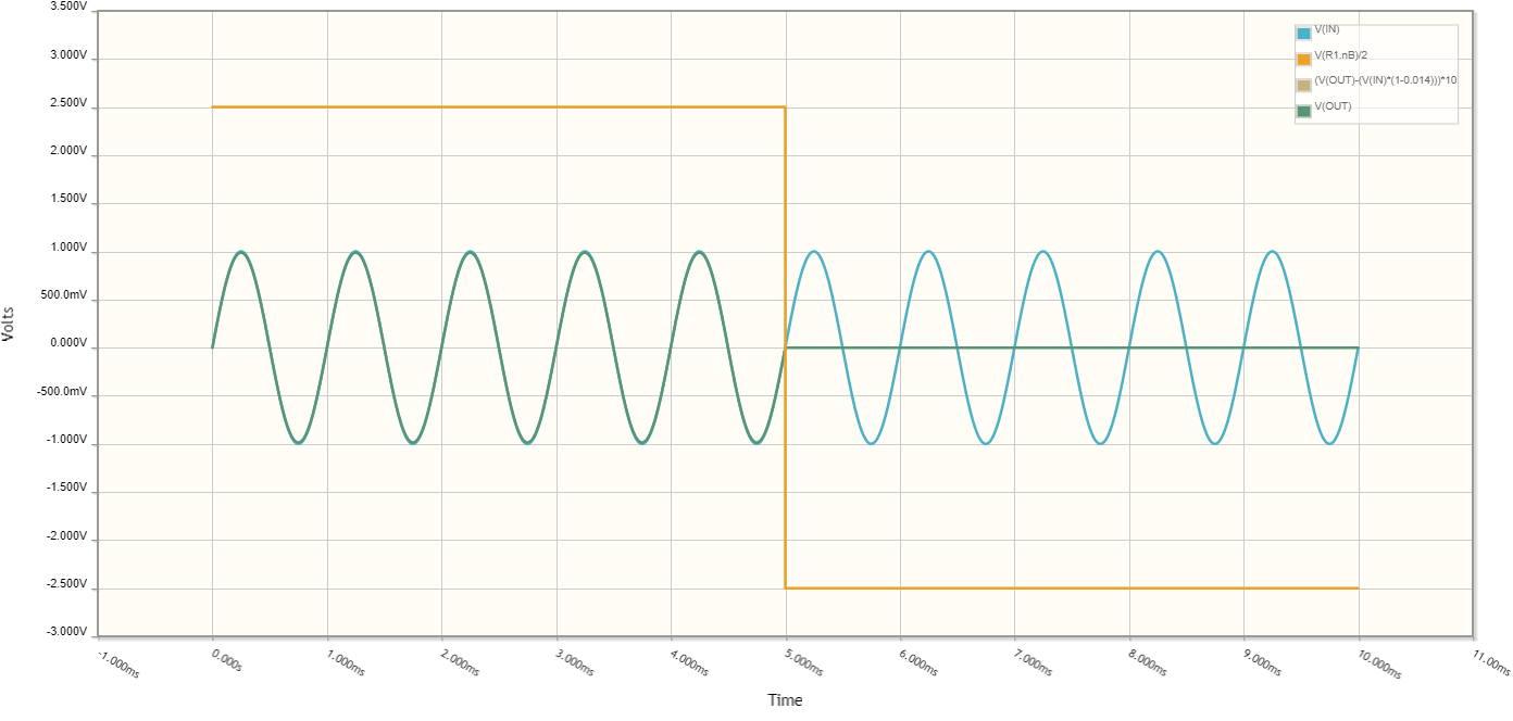
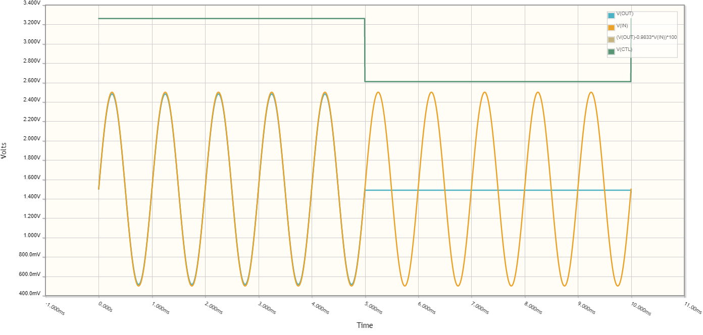
Below are the input, output and control waveforms of the circuit above. The control waveform's amplitude is scaled down 50% to make it fit better in the plot.
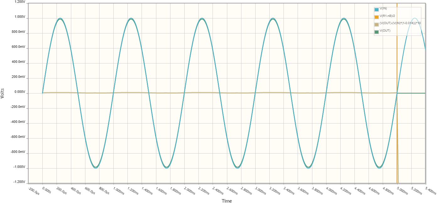
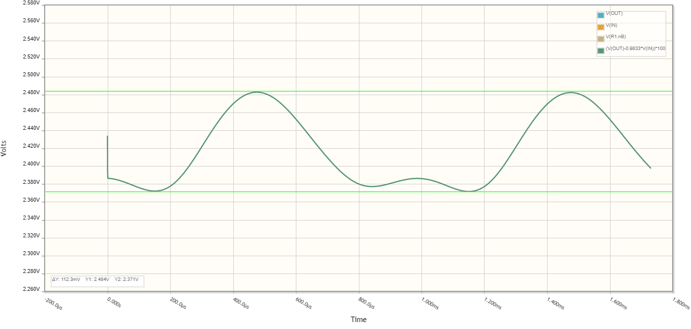
The non-linear distortion is about 0.5%. The input, output and distortion residue waveforms are plotted below.
The output isolation at 1kHz in the off state is beyond the fidelity of CircuitLab, presumably better than -70dB - this can depend a lot on the transistor used as well.
Another way to achieve a switching action would be to short a high-impedance source.
For example:
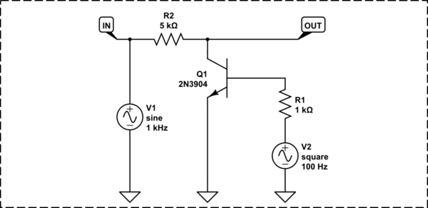
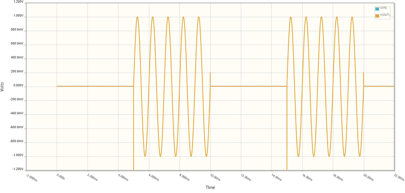
The output swings to 0V when it's turned off:
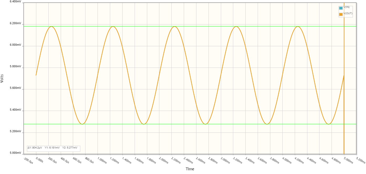
The isolation when OFF is about -66dB, or about 1-in-2000.
A more dependable way to implement a bipolar switch would be to convert the input signal to a current, then switch the current between two resistors, and take the output from one resistor only.
The switching action is clean:
The distortion residuals are <0.1%:
A practical realization of the switch circuit requires a voltage-current converter (V🠖I), and a source of bias currents, shown below.
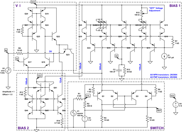
The various currents are derived from a 100uA reference. An LM334 could generate this current, for example. Another option would be REF200, but it costs an order of magnitude more.
The V🠖I converter maintains 3V at the emitter of Q23, and uses R8 to load input voltage using 3V as the reference. The current passes through Q23.
The current then gets subtracted from the 300uA reference, and enters the Q1-Q2 current steering pair. When the switch is turned on, Q2 conducts and passes the current through the output load resistor R5.
The voltage gain of the switch is about 0.983. Both the input and output impedance are 10 kOhm.
The switching action waveforms are below.
Distortion is under 0.1%. As shown below, it is about 0.06% at 1kHz.
OFF isolation at 1kHz is -90dB according to CircuitLab. In practice I'd expect -80dB at least with careful layout.
Given the relatively high output impedance, the output would need a buffer stage.
Lower distortion can be achieved by running the switch at a lower gain, say 0.2, and having the buffer stage add the gain back.
The V-I converter could be done with an op-amp Howland current pump, but that would take good resistors and a good op-amp to be better than the discrete circuit. At 30kHz, you'd need an op-amp with GBW to 10MHz to maintain reasonable distortion, if you care about that.
An op-amp could provide the gain and buffering of the switch output, of course.

