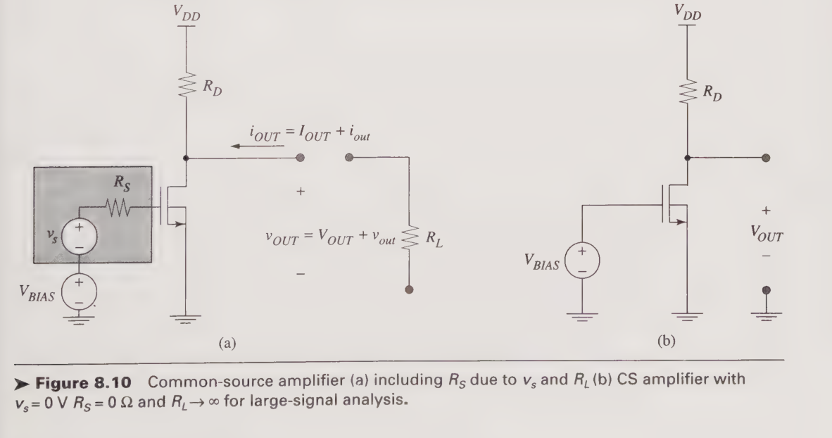
Im currently studying electronic devices. Ive reached transistor amplifiers. The image above shows a common-source amplifier. Im confused about why the textbook takes the load out for DC analysis. Wont the analysis be invalid after we connect the load back, wont conditions, eg, output voltage, change due to the re-connection of \$R_L\$? The textbook talks about how \$V_{BIAS}\$ vs \$V_{OUT}\$ is such that at about \$V_{DD}/2\$ the small-signal gain is the highest, using a plot that they present, which is fine, but how do I connect the open-circuit behaviour to the case where \$R_L\$ is actually there?
Edit: The image comes from page 475 of the following book,
title: Microelectronics: An integrated approach authors: Roger T. Howe & Charles G. Sodini publisher: Prentice Hall ISBN: 9780135885185

