34
\$\begingroup\$

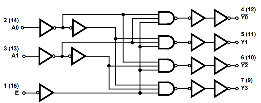
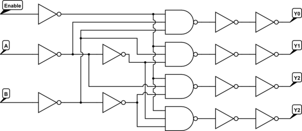
I have recently been looking at the datasheets for the 74HC139 IC in order to see if it was suitable for my project, and have come across the following logic diagram which strikes me as a little bit odd:
schematic

simulate this circuit – Schematic created using CircuitLab

For each of the inputs Yn, there are two NOT gates after the triple-input NAND gate; I don't understand why this is necessary as simple boolean logic tells us:

$$\overline{\overline{A}}\equiv A\qquad \forall A \in \{\text{TRUE}, \text{FALSE}\}$$

Therefore I am assuming there is some electronic based reason why there are two inverters before the output? I have heard not gates called Inverting buffers before, and these supposedly isolate the circuit before and after, however, I cannot claim to understand the use of this so I'd appreciate any enlightenment!

\$\endgroup\$

7 Answers 7

30
\$\begingroup\$

Possible reasons:

  1. Load Balancing
    • The driver of A has an unknown number of fan-out to drive. Fan-out within the circuit and the parasitic it induces can be calculated for the specific circuits, but we do not know the other circuits that are connected the driver. Essentially the inverters are being used as buffer equivalent. and help manage the parasitic.
  2. Timing and total current
    • To reduce the transition glitch, the second state inverters can be sized for a faster transition switch. Doing so makes the NAND gates input update near the same time. With the inputs changing less periodically, power can be saved and transition glitches can be reduced.
  3. Signal boosting and power
    • Lets say VDD = 1.2V but the input is 0.9V. The input is still a logical 1, but considered weak which causes slower switching and burns more power. The first inverters can be sized to handle transitions better, making the voltage more predictable for the rest of the design.
    • There is also a possibility of the change in the voltage domain. In this case the inverters in the first state can act as a step down, e.g. a 5V input domain to 2V domain.
  4. Any combination of the above
\$\endgroup\$
2
  • \$\begingroup\$ Thank you for your thorough answer, but what do you mean by the "parasitic"? \$\endgroup\$ Commented Apr 2, 2014 at 18:51
  • 2
    \$\begingroup\$ Parasitic can come in the from of capacitances, resistances and inductances. They are not part of the intended design and are a caused device/material physics. \$\endgroup\$
    – Greg
    Commented Apr 2, 2014 at 19:15
11
\$\begingroup\$

The time required for a gate to switch is dependent upon the amount of capacitive load it must drive, the size of the transistors, and the number of transistors in series. An inverter consists of one NFET (N-channel Field Effect Transistor) and one PFET (P-channel FET); a three-input NAND gate has three PFETs in parallel and three NFETs in series. In order for a 3-input NAND gate to switch an output low as quickly as could an inverter, each of the three NFETs would have to be three times as big as would be the single NFET of an inverter.

For a small chip such as this one, the only transistors which have to drive any significant load are those connected to output pins. Using four outputs driven by inverters, it will be necessary to have four big PFETs and four big NFETs, plus a bunch of little ones. If one assigns the NFETs an area of "1", the PFETs would probably have an area of about 1.5 (P-channel material doesn't work quite as well as N-channel), for a total area of about 10. If the outputs were driven directly by NAND gates, it would be necessary to use twelve big PFETs (total area 18) and twelve huge NFETs (total area 36, for a total area of about 54. Adding 20 little NFETs and 20 little PFETs [12 each for the NAND, and 8 each for inverters] the circuit will reduce the area consumed by big transistors by 44 units-more than 80%!

Although there are some occasions when an output pin will be driven directly by a "logic gate" other than an inverter, driving outputs in such a fashion increases greatly the area required for output transistors; it's generally only worthwhile in cases where e.g. a device has two power-supply inputs and it must be able to drive its output low even when only one supply is working.

\$\endgroup\$
8
\$\begingroup\$

If the NAND gate is made in the obvious way (three parallel transistors to GND and three series transistors to Vdd) then it will have low source capability, the transitions will not be sharp, and the delay time will be load capacitance dependent. Adding a buffer (or two to restore the logic) cleans up all those problems.

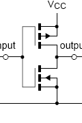
Here is what a typical unbuffered inverter (schematic like this)...

enter image description here

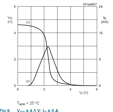
..transfer function (output vs. input shown on line (1)) looks like:

enter image description here

With a buffer, the line (1) will be much closer to a square shape. (the second line is the current that is drawn).

\$\endgroup\$
5
\$\begingroup\$

This is silly if you are just trying to communicate the logic of a chip. Probably it is drawn this way because internally there are some buffering stages. The internal gates are probably very small with little drive capability. Signals that go outside need to go thru a buffer that can source and sink much more current. Somehow this implementation detail seems to have made it into the logical description, where it doesn't belong. The logic would be the same if the two inverters in series were replaced by a wire. Then there should be a overall speed and current drive spec for the outputs. You could just as well envision slower and more powerful NAND gates.

\$\endgroup\$
3
  • 3
    \$\begingroup\$ The datasheet talks about typical propagation delay, in terms of "delay" units (e.g. "5 delays" from select to output). I imagine this is the reason for them drawing the logic diagram as so (to visualize what is causing the delays themselves). \$\endgroup\$
    – Shamtam
    Commented Apr 2, 2014 at 17:56
  • \$\begingroup\$ If the NAND gates drove the output directly, one might reasonably wonder whether the rising-edge speed would be affected by how many NAND inputs were low. Likewise, if some NAND inputs connected directly to input pins, one might reasonably wonder whether the switching threshold would be affected by the states of other inputs. Having each input feed one inverter, and each output fed by one inverter, implies that such effects are unlikely to occur to any significant degree. \$\endgroup\$
    – supercat
    Commented Apr 3, 2014 at 15:04
  • \$\begingroup\$ @supe: I don't expect logic diagrams in datasheets to be the exact logic as layed out on the chip, but rather only to show me conceptually what the chip does. Many datasheets even come right out and say that. Unless a datasheet explicitly said the contrary, that's what I'd assume, and therefore not make any assumptions about speed, drive level, and the like beyond the numbers in the datasheet. \$\endgroup\$ Commented Apr 3, 2014 at 15:07
3
\$\begingroup\$

While this may seem like a pointless thing to do, it does have practical application. This will boost the weak output signal. The level is unchanged, but the full current sourcing or sinking capabilities of final inverter are available to drive a load resistance if needed

\$\endgroup\$
3
\$\begingroup\$

In the past, such arrangement was used for a delay.

\$\endgroup\$
1
  • 6
    \$\begingroup\$ The insight, which you have posted is useful. At the same time, a short post like this would work better as a comment than as an answer. \$\endgroup\$ Commented Apr 2, 2014 at 18:54
0
\$\begingroup\$

From HCMOS family characteristics:

The 74HC/HCT/HCU high-speed Si-gate CMOS logic family combines the low power advantages of the HE4000B family with the high speed and drive capability of the low power Schottky TTL (LSTTL).

Internally, 4000 CMOS with final stage as 74LS compatible. Simplest CMOS gate (in 1988) is a NOT gate, so that is the only gate requiring low power Schottky TTL output compatibility. Standard Outputs: 10 LSTTL Loads. Benefits of CMOS speed, but capable of 5V TTL operation.

A cross-over family by Philips between TTL and CMOS. Back when TTL reigned because it was the fastest, but before TTL was dropped because TTL gates always draw power.

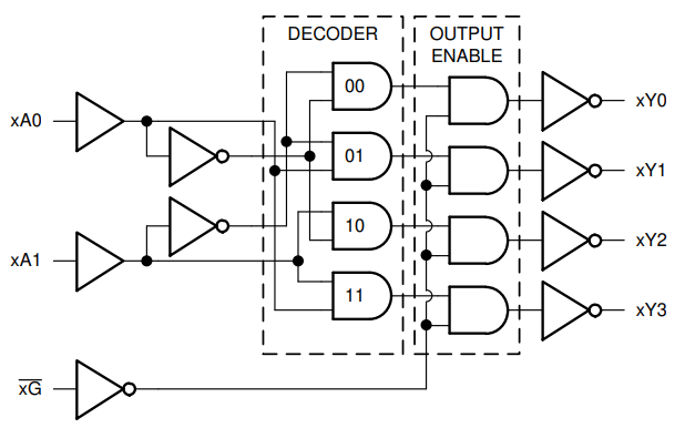
I prefer the TI 74HC139 datasheet schematic with deMorgan symbols. Output on NAND is active low, so double inverter to buffer active low outputs. The last inverter would not have the same physical layout as the previous.

enter image description here

All 74HC chips would have an inverter or buffer to provide low power Schottky TTL output compatibility. That would include NANDs and NORs.

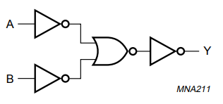
From Philips Quad 2-input NAND gate: 74HC00 Data sheet:

enter image description here

Positive NAND represented by a deMorgan's negative OR.

Double inverters have a bigger propagation delay, but probably a design trade off by the Philips designers in 1988. It was included on initial versions by TI as shown above but eliminated on latest revision by TI to decrease propagation delays.

enter image description here

\$\endgroup\$

Your Answer

By clicking “Post Your Answer”, you agree to our terms of service and acknowledge you have read our privacy policy.

Not the answer you're looking for? Browse other questions tagged or ask your own question.