D2 was not in reverse bias.
Source Link
Allenph
  • 737
  • 4
  • 13
  • 32

schematicschematic

simulate this circuitsimulate this circuit – Schematic created using CircuitLab

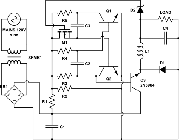
This is my rough sketch for a buck converter controlled by a BJT based astable multi-vibrator with zener-based feedback. Before I go through getting the values of each component, I wanted to make sure that I understand how these components would work in my circuit, and if I've done anything dangerous here.

Theory of Operation:

  1. The mains go through a transformer which brings it down to 20-25V AC. This also has the effect of isolating the circuit from earth-ground.
  2. The bridge rectifier BR1 converts the AC into full-wave DC.
  3. C1 is a giant electrolytic which smoothes the DC wave into "constant" DC.

Oscillator:

  1. R1 and R2 form a voltage divider which provides 5V to the oscillator. It is acceptable to use a voltage divider because the load of the oscillator will be known, and the current it draws will be relatively low. Our efficiency is not completely compromised due to this, and we don't get an unmanageable production of heat.
  2. The 5V is fed into a standard BJT astable oscillator, with one exception. The low-value resistor which dictates the RC time constant of C3 is replaced by a P-Type Mosfet which acts as a variable resistor. Variation in the current on the gate of the Mosfet will change the RC time constant of C3, effectively modulating out pulse width if we apply feedback.
  3. The collector of Q2 is used as the input to our buck converter.
  4. D2 is a reverse bias zener diode. If the voltage goes above 12V then the zener will allow current through. This current will be sent to the gate of M1, the "variable resistor" Mosfet from step 2. D2 is placed in reverse bias directly to the load. This channel is used as feedback.

Buck Converter:

  1. An NPN BJT (Q3) is being used as a switch. Since we're dealing with 5V logic, saturation shouldn't be an issue.
  2. L1 evens out changes in current, while C4 evens out changes in voltage. This averages the input.
  3. D1 prevents a massive negative voltage surge from destroying the BJT switch Q3 when Q3 goes from on to off.

Question:
Is there anything wrong with the theoretical version of the circuit, barring that it needs to have values applied to the components?

schematic

simulate this circuit – Schematic created using CircuitLab

This is my rough sketch for a buck converter controlled by a BJT based astable multi-vibrator with zener-based feedback. Before I go through getting the values of each component, I wanted to make sure that I understand how these components would work in my circuit, and if I've done anything dangerous here.

Theory of Operation:

  1. The mains go through a transformer which brings it down to 20-25V AC. This also has the effect of isolating the circuit from earth-ground.
  2. The bridge rectifier BR1 converts the AC into full-wave DC.
  3. C1 is a giant electrolytic which smoothes the DC wave into "constant" DC.

Oscillator:

  1. R1 and R2 form a voltage divider which provides 5V to the oscillator. It is acceptable to use a voltage divider because the load of the oscillator will be known, and the current it draws will be relatively low. Our efficiency is not completely compromised due to this, and we don't get an unmanageable production of heat.
  2. The 5V is fed into a standard BJT astable oscillator, with one exception. The low-value resistor which dictates the RC time constant of C3 is replaced by a P-Type Mosfet which acts as a variable resistor. Variation in the current on the gate of the Mosfet will change the RC time constant of C3, effectively modulating out pulse width if we apply feedback.
  3. The collector of Q2 is used as the input to our buck converter.
  4. D2 is a reverse bias zener diode. If the voltage goes above 12V then the zener will allow current through. This current will be sent to the gate of M1, the "variable resistor" Mosfet from step 2. D2 is placed in reverse bias directly to the load. This channel is used as feedback.

Buck Converter:

  1. An NPN BJT (Q3) is being used as a switch. Since we're dealing with 5V logic, saturation shouldn't be an issue.
  2. L1 evens out changes in current, while C4 evens out changes in voltage. This averages the input.
  3. D1 prevents a massive negative voltage surge from destroying the BJT switch Q3 when Q3 goes from on to off.

Question:
Is there anything wrong with the theoretical version of the circuit, barring that it needs to have values applied to the components?

added 225 characters in body
Source Link
Allenph
  • 737
  • 4
  • 13
  • 32
 

Circuit Diagramschematic

simulate this circuit – Schematic created using CircuitLab

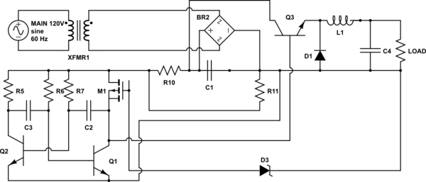
This is my rough sketch for a buck converter controlled by a BJT based astable multi-vibrator with zener-based feedback. Before I go through getting the values of each component, I wanted to make sure that I understand how these components would work in my circuit, and if I've done anything dangerous here.

Theory of Operation:

  1. The mains go through a transformer which brings it down to 20-25V AC. This also has the effect of isolating the circuit from earth-ground.
  2. The bridge rectifier BR2BR1 converts the AC into full-wave DC.
  3. C1 is a giant electrolytic which smoothes the DC wave into "constant" DC.

Oscillator:

  1. R10R1 and R11R2 form a voltage divider which provides 5V to the oscillator. It is acceptable to use a voltage divider because the load of the oscillator will be known, and the current it draws will be relatively low. Our efficiency is not completely compromised due to this, and we don't get an unmanageable production of heat.
  2. The 5V is fed into a standard BJT astable oscillator, with one exception. The low-value resistor which dictates the RC time constant of C2C3 is replaced by a P-Type Mosfet which acts as a variable resistor. VariatingVariation in the current on the gate of the Mosfet will change the RC time constant of C2C3, effectively modulating out pulse width if we apply feedback.
  3. The collector of Q1Q2 is used as the input to our buck converter.
  4. D3D2 is a reverse bias zener diode. If the voltage goes above 12V then the zener will allow current through. This current will be sent to the gate of M1, the "variable resistor" Mosfet from step 2. D3 D2 is placed in reverse bias directly to the load. This channel is used as feedback.

Buck Converter:

  1. An NPN BJT (Q3) is being used as a switch. Since we're dealing with 5V logic, saturation shouldn't be an issue.
  2. L1 evens out changes in current, while C4 evens out changes in voltage. This averages the input.
  3. D1 prevents a massive negative voltage surge from destroying the BJT switch Q3 when Q3 isgoes from on to off.

Question:
Is there anything wrong with the theoretical version of the circuit, barring that it needs to have values applied to the components?

Circuit Diagram

This is my rough sketch for a buck converter controlled by a BJT based astable multi-vibrator with zener-based feedback. Before I go through getting the values of each component, I wanted to make sure that I understand how these components would work in my circuit, and if I've done anything dangerous here.

Theory of Operation:

  1. The mains go through a transformer which brings it down to 20-25V AC. This also has the effect of isolating the circuit from earth-ground.
  2. The bridge rectifier BR2 converts the AC into full-wave DC.
  3. C1 is a giant electrolytic which smoothes the DC wave into "constant" DC.

Oscillator:

  1. R10 and R11 form a voltage divider which provides 5V to the oscillator. It is acceptable to use a voltage divider because the load of the oscillator will be known, and the current it draws will be relatively low. Our efficiency is not completely compromised due to this, and we don't get an unmanageable production of heat.
  2. The 5V is fed into a standard BJT astable oscillator, with one exception. The low-value resistor which dictates the RC time constant of C2 is replaced by a P-Type Mosfet which acts as a variable resistor. Variating the current on the gate of the Mosfet will change the RC time constant of C2, effectively modulating out pulse width if we apply feedback.
  3. The collector of Q1 is used as the input to our buck converter.
  4. D3 is a reverse bias zener diode. If the voltage goes above 12V then the zener will allow current through. This current will be sent to M1, the "variable resistor" Mosfet from step 2. D3 is placed in reverse bias directly to the load. This channel is used as feedback.

Buck Converter:

  1. An NPN BJT is being used as a switch. Since we're dealing with 5V logic, saturation shouldn't be an issue.
  2. L1 evens out changes in current, while C4 evens out changes in voltage. This averages the input.
  3. D1 prevents a massive negative voltage surge from destroying the BJT switch Q3 when Q3 is off.

Question:
Is there anything wrong with the theoretical version of the circuit, barring that it needs to have values applied to the components?


schematic

simulate this circuit – Schematic created using CircuitLab

This is my rough sketch for a buck converter controlled by a BJT based astable multi-vibrator with zener-based feedback. Before I go through getting the values of each component, I wanted to make sure that I understand how these components would work in my circuit, and if I've done anything dangerous here.

Theory of Operation:

  1. The mains go through a transformer which brings it down to 20-25V AC. This also has the effect of isolating the circuit from earth-ground.
  2. The bridge rectifier BR1 converts the AC into full-wave DC.
  3. C1 is a giant electrolytic which smoothes the DC wave into "constant" DC.

Oscillator:

  1. R1 and R2 form a voltage divider which provides 5V to the oscillator. It is acceptable to use a voltage divider because the load of the oscillator will be known, and the current it draws will be relatively low. Our efficiency is not completely compromised due to this, and we don't get an unmanageable production of heat.
  2. The 5V is fed into a standard BJT astable oscillator, with one exception. The low-value resistor which dictates the RC time constant of C3 is replaced by a P-Type Mosfet which acts as a variable resistor. Variation in the current on the gate of the Mosfet will change the RC time constant of C3, effectively modulating out pulse width if we apply feedback.
  3. The collector of Q2 is used as the input to our buck converter.
  4. D2 is a reverse bias zener diode. If the voltage goes above 12V then the zener will allow current through. This current will be sent to the gate of M1, the "variable resistor" Mosfet from step 2. D2 is placed in reverse bias directly to the load. This channel is used as feedback.

Buck Converter:

  1. An NPN BJT (Q3) is being used as a switch. Since we're dealing with 5V logic, saturation shouldn't be an issue.
  2. L1 evens out changes in current, while C4 evens out changes in voltage. This averages the input.
  3. D1 prevents a massive negative voltage surge from destroying the BJT switch Q3 when Q3 goes from on to off.

Question:
Is there anything wrong with the theoretical version of the circuit, barring that it needs to have values applied to the components?

edited body
Source Link
Allenph
  • 737
  • 4
  • 13
  • 32

Circuit Diagram

This is my rough sketch for a buck converter controlled by a BJT based astable multi-vibrator with zener-based feedback. Before I go through getting the values of each component, I wanted to make sure that I understand how these components would work in my circuit, and if I've done anything dangerous here.

Theory of Operation:

  1. The mains go through a transformer which brings it down to 20-25V AC. This also has the effect of isolating the circuit from earth-ground.
  2. The bridge rectifier BR2 converts the AC into full-wave DC.
  3. C1 is a giant electrolytic which smoothes the DC wave into "constant" DC.

Oscillator:

  1. R10 and R11 form a voltage divider which provides 5V to the oscillator. It is acceptable to use a voltage divider because the load of the oscillator will be known, and the current it draws will be relatively low. Our efficiency is not completely compromised due to this, and we don't get an unmanageable production of heat.
  2. The 5V is fed into a standard BJT astable oscillator, with one exception. The low-value resistor which dictates the RC time constant of C2 is replaced by a P-Type Mosfet which acts as a variable resistor. Variating the current on the gate of the Mosfet will change the RC time constant of C2, effectively modulating out pulse width if we apply feedback.
  3. The collector of Q1 is used as the input to our buck converter.
  4. D3 is a reverse bias zener diode. If the currentvoltage goes above 12V then the zener will allow current through. This current will be sent to M1, the "variable resistor" Mosfet from step 2. D3 is placed in reverse bias directly to the load. This channel is used as feedback.

Buck Converter:

  1. An NPN BJT is being used as a switch. Since we're dealing with 5V logic, saturation shouldn't be an issue.
  2. L1 evens out changes in current, while C4 evens out changes in voltage. This averages the input.
  3. D1 prevents a massive negative voltage surge from destroying the BJT switch Q3 when Q3 is off.

Question:
Is there anything wrong with the theoretical version of the circuit, barring that it needs to have values applied to the components?

Circuit Diagram

This is my rough sketch for a buck converter controlled by a BJT based astable multi-vibrator with zener-based feedback. Before I go through getting the values of each component, I wanted to make sure that I understand how these components would work in my circuit, and if I've done anything dangerous here.

Theory of Operation:

  1. The mains go through a transformer which brings it down to 20-25V AC. This also has the effect of isolating the circuit from earth-ground.
  2. The bridge rectifier BR2 converts the AC into full-wave DC.
  3. C1 is a giant electrolytic which smoothes the DC wave into "constant" DC.

Oscillator:

  1. R10 and R11 form a voltage divider which provides 5V to the oscillator. It is acceptable to use a voltage divider because the load of the oscillator will be known, and the current it draws will be relatively low. Our efficiency is not completely compromised due to this, and we don't get an unmanageable production of heat.
  2. The 5V is fed into a standard BJT astable oscillator, with one exception. The low-value resistor which dictates the RC time constant of C2 is replaced by a P-Type Mosfet which acts as a variable resistor. Variating the current on the gate of the Mosfet will change the RC time constant of C2, effectively modulating out pulse width if we apply feedback.
  3. The collector of Q1 is used as the input to our buck converter.
  4. D3 is a reverse bias zener diode. If the current goes above 12V then the zener will allow current through. This current will be sent to M1, the "variable resistor" Mosfet from step 2. D3 is placed in reverse bias directly to the load. This channel is used as feedback.

Buck Converter:

  1. An NPN BJT is being used as a switch. Since we're dealing with 5V logic, saturation shouldn't be an issue.
  2. L1 evens out changes in current, while C4 evens out changes in voltage. This averages the input.
  3. D1 prevents a massive negative voltage surge from destroying the BJT switch Q3 when Q3 is off.

Question:
Is there anything wrong with the theoretical version of the circuit, barring that it needs to have values applied to the components?

Circuit Diagram

This is my rough sketch for a buck converter controlled by a BJT based astable multi-vibrator with zener-based feedback. Before I go through getting the values of each component, I wanted to make sure that I understand how these components would work in my circuit, and if I've done anything dangerous here.

Theory of Operation:

  1. The mains go through a transformer which brings it down to 20-25V AC. This also has the effect of isolating the circuit from earth-ground.
  2. The bridge rectifier BR2 converts the AC into full-wave DC.
  3. C1 is a giant electrolytic which smoothes the DC wave into "constant" DC.

Oscillator:

  1. R10 and R11 form a voltage divider which provides 5V to the oscillator. It is acceptable to use a voltage divider because the load of the oscillator will be known, and the current it draws will be relatively low. Our efficiency is not completely compromised due to this, and we don't get an unmanageable production of heat.
  2. The 5V is fed into a standard BJT astable oscillator, with one exception. The low-value resistor which dictates the RC time constant of C2 is replaced by a P-Type Mosfet which acts as a variable resistor. Variating the current on the gate of the Mosfet will change the RC time constant of C2, effectively modulating out pulse width if we apply feedback.
  3. The collector of Q1 is used as the input to our buck converter.
  4. D3 is a reverse bias zener diode. If the voltage goes above 12V then the zener will allow current through. This current will be sent to M1, the "variable resistor" Mosfet from step 2. D3 is placed in reverse bias directly to the load. This channel is used as feedback.

Buck Converter:

  1. An NPN BJT is being used as a switch. Since we're dealing with 5V logic, saturation shouldn't be an issue.
  2. L1 evens out changes in current, while C4 evens out changes in voltage. This averages the input.
  3. D1 prevents a massive negative voltage surge from destroying the BJT switch Q3 when Q3 is off.

Question:
Is there anything wrong with the theoretical version of the circuit, barring that it needs to have values applied to the components?

added 2 characters in body
Source Link
Allenph
  • 737
  • 4
  • 13
  • 32
Loading
Source Link
Allenph
  • 737
  • 4
  • 13
  • 32
Loading