added 390 characters in body
Source Link
jbord39
  • 4.4k
  • 1
  • 19
  • 25

When you say edge triggered it sort of implies a clock edge. People are seeing this and forcing a clock signal somehow. But in your description you just describe two inputs which are triggered on the rising edge and ignore falling edges.

This is a similar situation to MS-CMOS, where the capture latches are implemented using SR. In MS-CMOS, it is always guaranteed that ONE of the S or R signals will rise and fall; and the other will not. So an SR latch suffices.

You also did not constrain whether after one signal rises, it will fall before the next. I will assume that this is not the case, and that if Signal1 rises and sets output to 1, and before Signal1 falls, Signal2 rises; that it should set the output to 0.

I believe you are looking for a SR NOR latch, modified to toggle in the S=R=1 state. This is often called a JK latch.

Lets call J = S1 = "one input would, on rising edge, set the output to 1"
Lets call K = S2 = "and the other input would, on rising edge, set the output to 0"

Both J and R = 0 to begin. Output state is indeterminate.

Then, J rises. This sets Q = 1.
Next, J falls. The output stays 1.
Next, K rises. The output is set to 0.
Next, K falls. The output stays 0.
Next, J rises. The output is set to 1.
Next, K rises. The output is set to 0. (this is JK toggle state, if this won't happen just use NOR SR latch)
Next, J falls. The output stays 0.
Next, K falls. The output stays 0.
...

Is this what you are looking for? Wiki link, showing truth table, gate level schematic

EDIT: Added fix for both inputs @ 1 simultaneously.

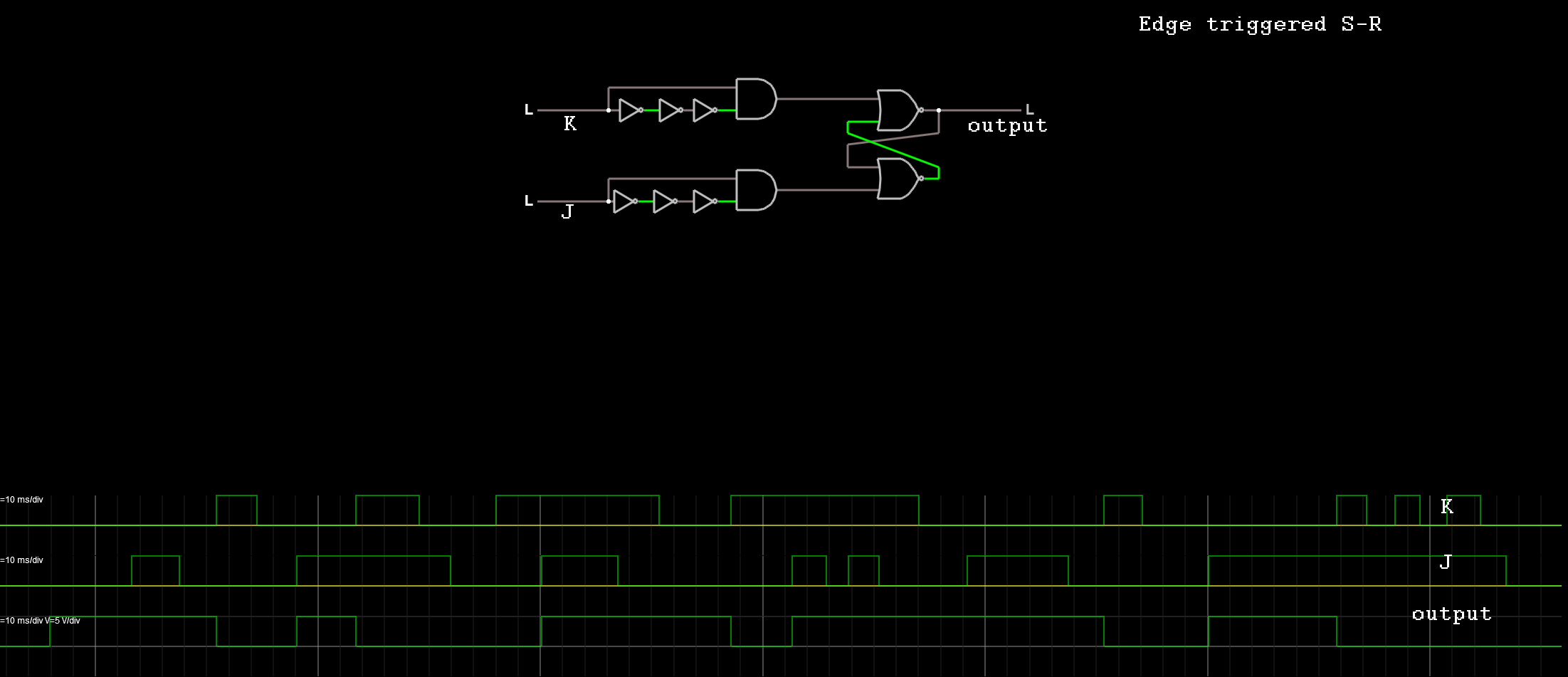
If you want both edges at once to toggle, generate a pulse to clock the flip flop. The pulse duration needs to be wide enough to toggle once but not twice. 1 or 3 inverters should work; I chose 3 in this case. The simple simulator didn't have 3 input ANDs so I just chained two 2-inputs back to back; either will work.

showing schematic and simulation results

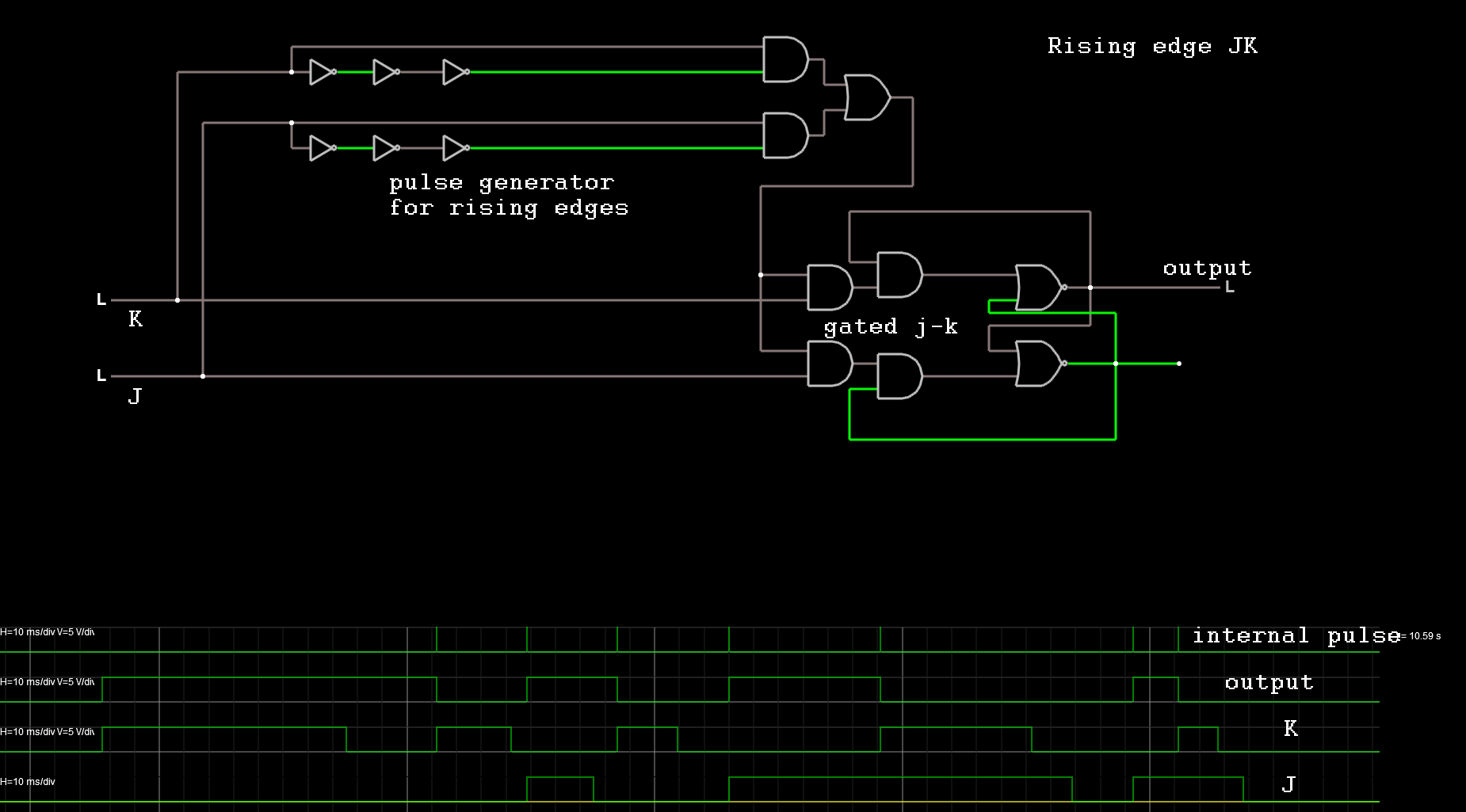
Edit2: Dave Tweed pointed out that holding one input high and repeatedly pulsing the other would toggle each time. Also he suggested combining SR with the pulse detectors. I have attached schematic and simulation below.

It is quite lean and low power/small (only 10 gates).

updated sr latch w/ rising edge pulse generators

It will have indeterminate state if both inputs rise simultaneously (within the pulse width duration). Other implementations will have a similar effect to lesser or greater degree depending on the topology.

When you say edge triggered it sort of implies a clock edge. People are seeing this and forcing a clock signal somehow. But in your description you just describe two inputs which are triggered on the rising edge and ignore falling edges.

This is a similar situation to MS-CMOS, where the capture latches are implemented using SR. In MS-CMOS, it is always guaranteed that ONE of the S or R signals will rise and fall; and the other will not. So an SR latch suffices.

You also did not constrain whether after one signal rises, it will fall before the next. I will assume that this is not the case, and that if Signal1 rises and sets output to 1, and before Signal1 falls, Signal2 rises; that it should set the output to 0.

I believe you are looking for a SR NOR latch, modified to toggle in the S=R=1 state. This is often called a JK latch.

Lets call J = S1 = "one input would, on rising edge, set the output to 1"
Lets call K = S2 = "and the other input would, on rising edge, set the output to 0"

Both J and R = 0 to begin. Output state is indeterminate.

Then, J rises. This sets Q = 1.
Next, J falls. The output stays 1.
Next, K rises. The output is set to 0.
Next, K falls. The output stays 0.
Next, J rises. The output is set to 1.
Next, K rises. The output is set to 0. (this is JK toggle state, if this won't happen just use NOR SR latch)
Next, J falls. The output stays 0.
Next, K falls. The output stays 0.
...

Is this what you are looking for? Wiki link, showing truth table, gate level schematic

EDIT: Added fix for both inputs @ 1 simultaneously.

If you want both edges at once to toggle, generate a pulse to clock the flip flop. The pulse duration needs to be wide enough to toggle once but not twice. 1 or 3 inverters should work; I chose 3 in this case. The simple simulator didn't have 3 input ANDs so I just chained two 2-inputs back to back; either will work.

showing schematic and simulation results

Edit2: Dave Tweed pointed out that holding one input high and repeatedly pulsing the other would toggle each time. Also he suggested combining SR with the pulse detectors. I have attached schematic and simulation below.

It is quite lean and low power/small (only 10 gates).

updated sr latch w/ rising edge pulse generators

It will have indeterminate state if both inputs rise simultaneously (within the pulse width duration). Other implementations will have a similar effect to lesser or greater degree depending on the topology.
added 546 characters in body
Source Link
jbord39
  • 4.4k
  • 1
  • 19
  • 25

When you say edge triggered it sort of implies a clock edge. People are seeing this and forcing a clock signal somehow. But in your description you just describe two inputs which are triggered on the rising edge and ignore falling edges.

This is a similar situation to MS-CMOS, where the capture latches are implemented using SR. In MS-CMOS, it is always guaranteed that ONE of the S or R signals will rise and fall; and the other will not. So an SR latch suffices.

You also did not constrain whether after one signal rises, it will fall before the next. I will assume that this is not the case, and that if Signal1 rises and sets output to 1, and before Signal1 falls, Signal2 rises; that it should set the output to 0.

I believe you are looking for a SR NOR latch, modified to toggle in the S=R=1 state. This is often called a JK latch.

Lets call J = S1 = "one input would, on rising edge, set the output to 1"
Lets call K = S2 = "and the other input would, on rising edge, set the output to 0"

Both J and R = 0 to begin. Output state is indeterminate.

Then, J rises. This sets Q = 1.
Next, J falls. The output stays 1.
Next, K rises. The output is set to 0.
Next, K falls. The output stays 0.
Next, J rises. The output is set to 1.
Next, K rises. The output is set to 0. (this is JK toggle state, if this won't happen just use NOR SR latch)
Next, J falls. The output stays 0.
Next, K falls. The output stays 0.
...

Is this what you are looking for? Wiki link, showing truth table, gate level schematic

EDIT: Added fix for both inputs @ 1 simultaneously.

If you want both edges at once to toggle, generate a pulse to clock the flip flop. The pulse duration needs to be less than the full J-K loop (feedforward NOR + feedback AND)wide enough to toggle once but more than the feedforward NOR delaynot twice. 1 or 3 inverters should work; I chose 3 in this case. The simple simulator didn't have 3 input ANDs so I just chained two 2-inputs back to back; either will work.

showing schematic and simulation results

When you say edge triggered it sort of implies a clock edge. People are seeing this and forcing a clock signal somehow. But in your description you just describe two inputs which are triggered on the rising edge and ignore falling edges.

This is a similar situation to MS-CMOS, where the capture latches are implemented using SR. In MS-CMOS, it is always guaranteed that ONE of the S or R signals will rise and fall; and the other will not. So an SR latch suffices.

You also did not constrain whether after one signal rises, it will fall before the next. I will assume that this is not the case, and that if Signal1 rises and sets output to 1, and before Signal1 falls, Signal2 rises; that it should set the output to 0.

I believe you are looking for a SR NOR latch, modified to toggle in the S=R=1 state. This is often called a JK latch.

Lets call J = S1 = "one input would, on rising edge, set the output to 1"
Lets call K = S2 = "and the other input would, on rising edge, set the output to 0"

Both J and R = 0 to begin. Output state is indeterminate.

Then, J rises. This sets Q = 1.
Next, J falls. The output stays 1.
Next, K rises. The output is set to 0.
Next, K falls. The output stays 0.
Next, J rises. The output is set to 1.
Next, K rises. The output is set to 0. (this is JK toggle state, if this won't happen just use NOR SR latch)
Next, J falls. The output stays 0.
Next, K falls. The output stays 0.
...

Is this what you are looking for? Wiki link, showing truth table, gate level schematic

EDIT: Added fix for both inputs @ 1 simultaneously.

If you want both edges at once to toggle, generate a pulse to clock the flip flop. The pulse duration needs to be less than the full J-K loop (feedforward NOR + feedback AND) but more than the feedforward NOR delay. 1 or 3 inverters should work; I chose 3 in this case. The simple simulator didn't have 3 input ANDs so I just chained two 2-inputs back to back; either will work.

showing schematic and simulation results

When you say edge triggered it sort of implies a clock edge. People are seeing this and forcing a clock signal somehow. But in your description you just describe two inputs which are triggered on the rising edge and ignore falling edges.

This is a similar situation to MS-CMOS, where the capture latches are implemented using SR. In MS-CMOS, it is always guaranteed that ONE of the S or R signals will rise and fall; and the other will not. So an SR latch suffices.

You also did not constrain whether after one signal rises, it will fall before the next. I will assume that this is not the case, and that if Signal1 rises and sets output to 1, and before Signal1 falls, Signal2 rises; that it should set the output to 0.

I believe you are looking for a SR NOR latch, modified to toggle in the S=R=1 state. This is often called a JK latch.

Lets call J = S1 = "one input would, on rising edge, set the output to 1"
Lets call K = S2 = "and the other input would, on rising edge, set the output to 0"

Both J and R = 0 to begin. Output state is indeterminate.

Then, J rises. This sets Q = 1.
Next, J falls. The output stays 1.
Next, K rises. The output is set to 0.
Next, K falls. The output stays 0.
Next, J rises. The output is set to 1.
Next, K rises. The output is set to 0. (this is JK toggle state, if this won't happen just use NOR SR latch)
Next, J falls. The output stays 0.
Next, K falls. The output stays 0.
...

Is this what you are looking for? Wiki link, showing truth table, gate level schematic

EDIT: Added fix for both inputs @ 1 simultaneously.

If you want both edges at once to toggle, generate a pulse to clock the flip flop. The pulse duration needs to be wide enough to toggle once but not twice. 1 or 3 inverters should work; I chose 3 in this case. The simple simulator didn't have 3 input ANDs so I just chained two 2-inputs back to back; either will work.

showing schematic and simulation results

added 546 characters in body
Source Link
jbord39
  • 4.4k
  • 1
  • 19
  • 25

When you say edge triggered it sort of implies a clock edge. People are seeing this and forcing a clock signal somehow. But in your description you just describe two inputs which are triggered on the rising edge and ignore falling edges.

This is a similar situation to MS-CMOS, where the capture latches are implemented using SR. In MS-CMOS, it is always guaranteed that ONE of the S or R signals will rise and fall; and the other will not. So an SR latch suffices.

You also did not constrain whether after one signal rises, it will fall before the next. I will assume that this is not the case, and that if Signal1 rises and sets output to 1, and before Signal1 falls, Signal2 rises; that it should set the output to 0.

I believe you are looking for a SR NOR latch, modified to toggle in the S=R=1 state. This is often called a JK latch.

Lets call J = S1 = "one input would, on rising edge, set the output to 1"
Lets call K = S2 = "and the other input would, on rising edge, set the output to 0"

Both J and R = 0 to begin. Output state is indeterminate.

Then, J rises. This sets Q = 1.
Next, J falls. The output stays 1.
Next, K rises. The output is set to 0.
Next, K falls. The output stays 0.
Next, J rises. The output is set to 1.
Next, K rises. The output is set to 0. (this is JK toggle state, if this won't happen just use NOR SR latch)
Next, J falls. The output stays 0.
Next, K falls. The output stays 0.
...

Is this what you are looking for? Wiki link, showing truth table, gate level schematic

EDIT: Added fix for both inputs @ 1 simultaneously.

If you want both edges at once to toggle, generate a pulse to clock the flip flop. The pulse duration needs to be less than the full J-K loop (feedforward NOR + feedback AND) but more than the feedforward NOR delay. 1 or 3 inverters should work; I chose 3 in this case. The simple simulator didn't have 3 input ANDs so I just chained two 2-inputs back to back; either will work.

showing schematic and simulation results

When you say edge triggered it sort of implies a clock edge. People are seeing this and forcing a clock signal somehow. But in your description you just describe two inputs which are triggered on the rising edge and ignore falling edges.

This is a similar situation to MS-CMOS, where the capture latches are implemented using SR. In MS-CMOS, it is always guaranteed that ONE of the S or R signals will rise and fall; and the other will not. So an SR latch suffices.

You also did not constrain whether after one signal rises, it will fall before the next. I will assume that this is not the case, and that if Signal1 rises and sets output to 1, and before Signal1 falls, Signal2 rises; that it should set the output to 0.

I believe you are looking for a SR NOR latch, modified to toggle in the S=R=1 state. This is often called a JK latch.

Lets call J = S1 = "one input would, on rising edge, set the output to 1"
Lets call K = S2 = "and the other input would, on rising edge, set the output to 0"

Both J and R = 0 to begin. Output state is indeterminate.

Then, J rises. This sets Q = 1.
Next, J falls. The output stays 1.
Next, K rises. The output is set to 0.
Next, K falls. The output stays 0.
Next, J rises. The output is set to 1.
Next, K rises. The output is set to 0. (this is JK toggle state, if this won't happen just use NOR SR latch)
Next, J falls. The output stays 0.
Next, K falls. The output stays 0.
...

Is this what you are looking for? Wiki link, showing truth table, gate level schematic

EDIT: Added fix for both inputs @ 1 simultaneously.

If you want both edges at once to toggle, generate a pulse to clock the flip flop. The pulse duration needs to be less than the full J-K loop (feedforward NOR + feedback AND) but more than the feedforward NOR delay. 1 or 3 inverters should work; I chose 3 in this case. The simple simulator didn't have 3 input ANDs so I just chained two 2-inputs back to back; either will work.

showing schematic and simulation results

deleted 16 characters in body
Source Link
jbord39
  • 4.4k
  • 1
  • 19
  • 25
Loading
added 59 characters in body
Source Link
jbord39
  • 4.4k
  • 1
  • 19
  • 25
Loading
Source Link
jbord39
  • 4.4k
  • 1
  • 19
  • 25
Loading