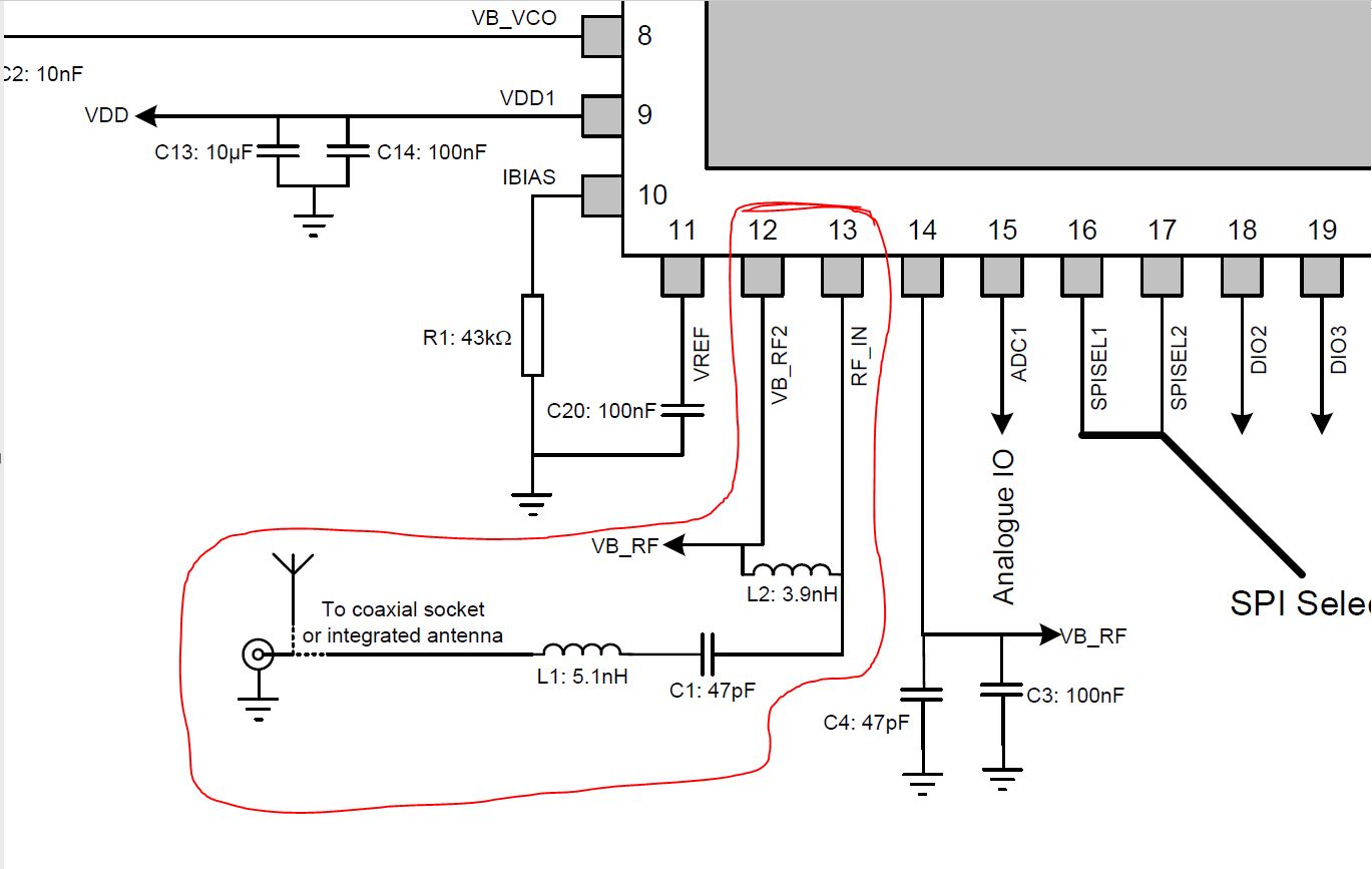
I am designing a PCB layout for NXP JN516x Wireless Microcontroller (http://www.nxp.com/docs/en/data-sheet/JN516X.pdf). Part of the design is the antenna, where I have to choose a 50ohm antenna. I decided to go with a chip antenna (https://www.digikey.com/product-detail/en/ethertronics-inc/1001312/939-1040-1-ND/4754415), since it has a small footprint. According to the NXP JN516X datasheet, There is a matching network for the antenna, as shown in the figure below (Page 89):
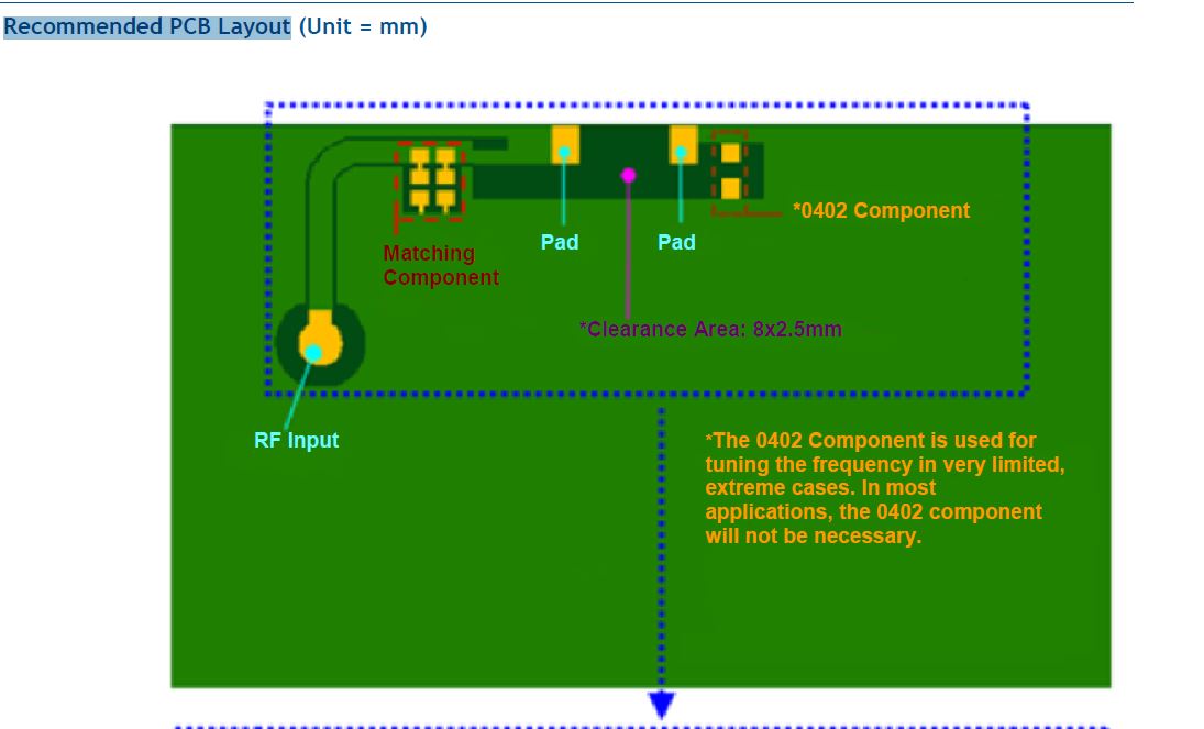
[![enter image description here][1]][1] But I can see from the datasheet of the antenna itself, there is a recommended PCB Layout, where it is clear in the below figure that there is only two matching components, and the datasheet didn't even mention anything about the values or whether they are inductors or capacitors.
[![enter image description here][2]][2]
I don't have much experience with antenna design. Which matching network should I use, the one in NXP datasheet or the one in the antenna datasheet?
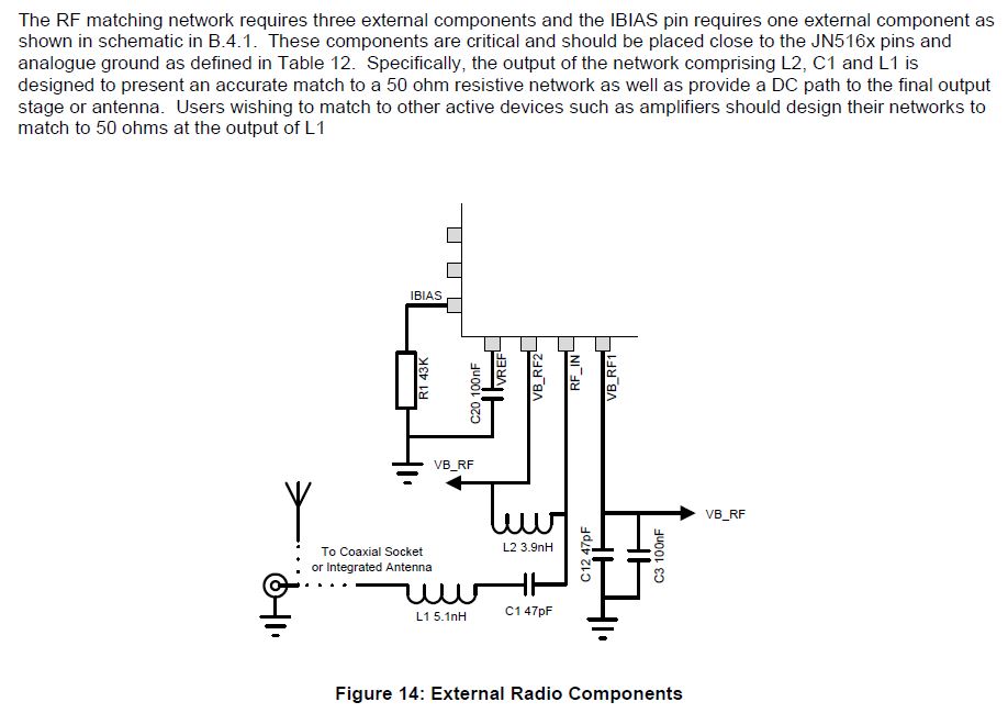
Update: I found the below statement on page 27 of the chip datasheet, it said that we need the three external components L1, L2 and C1, as they form a 50ohm resistive network. Does that mean I don't have to remove L1?
Thanks in advance.
What should I follow [1]: https://i.sstatic.net/Uuh6L.jpg [2]: https://i.sstatic.net/ZpU2R.jpg

