added 232 characters in body
Source Link
Gary
  • 43
  • 1
  • 6

Because I am a software dude, I would like some help verifying this minimal Arduino based circuit which I designed with some changes.

It is single AAA cell operated (NiCd or Alkaline), needs to be very energy efficient. Both ATMega and the DC Booster can be configured to any voltage between +1.8v to +5.5v, so I can go higher than +2.2v. Input: 4 push buttons, each can wake it up from sleep using Pin Change Interrupt on port D (All switches are pulled up internally). Once awake the circuit should read which switch woke it, A visible light Phototransistor whose analog value can be read. A tact switch whose on/off value can be read (pulled up internally). Output is done by blinking an LED using PWM. The software (including Arduino boot loader) needs to be burned over SPI using USBTinyISP. The FTDI port is for Arduino IDE debugging.

Are there errors in the attached design? Anything missing? Anything can be improved? enter image description here
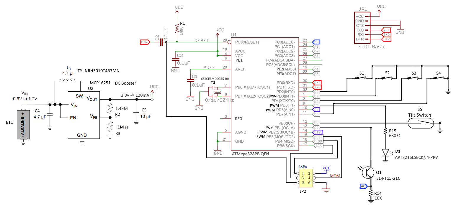
I ultimately built the circuit, and now have a problem with serial communication as described in this link.

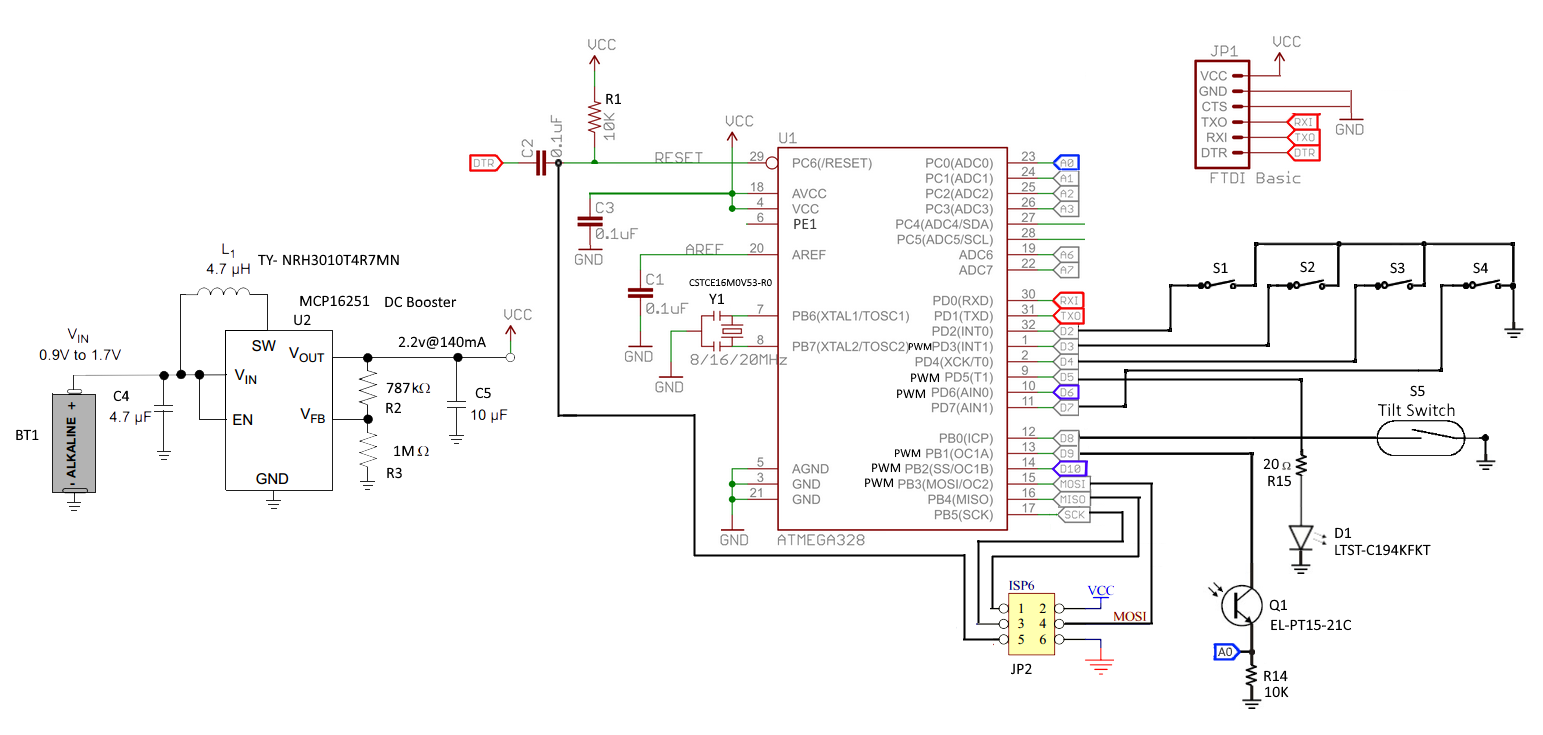
Because I am a software dude, I would like some help verifying this minimal Arduino based circuit which I designed with some changes.

It is single AAA cell operated (NiCd or Alkaline), needs to be very energy efficient. Both ATMega and the DC Booster can be configured to any voltage between +1.8v to +5.5v, so I can go higher than +2.2v. Input: 4 push buttons, each can wake it up from sleep using Pin Change Interrupt on port D (All switches are pulled up internally). Once awake the circuit should read which switch woke it, A visible light Phototransistor whose analog value can be read. A tact switch whose on/off value can be read (pulled up internally). Output is done by blinking an LED using PWM. The software (including Arduino boot loader) needs to be burned over SPI using USBTinyISP. The FTDI port is for Arduino IDE debugging.

Are there errors in the attached design? Anything missing? Anything can be improved? enter image description here

I ultimately built the circuit, and now have a problem with serial communication as described in this link.

Updated schematics with all recomendations
Source Link
Gary
  • 43
  • 1
  • 6

Because I am a software dude, I would like some help verifying this minimal Arduino based circuit which I designed with some changes.

It is single AAA cell operated (NiCd or Alkaline), needs to be very energy efficient. Both ATMega and the DC Booster can be configured to any voltage between +1.8v to +5.5v, so I can go higher than +2.2v. Input: 4 push buttons, each can wake it up from sleep using Pin Change Interrupt on port D (All switches are pulled up internally). Once awake the circuit should read which switch woke it, A visible light Phototransistor whose analog value can be read. A tact switch whose on/off value can be read (pulled up internally). Output is done by blinking an LED using PWM. The software (including Arduino boot loader) needs to be burned over SPI using USBTinyISP. The FTDI port is for Arduino IDE debugging.

Are there errors in the attached design? Anything missing? Anything can be improved? enter image description hereenter image description here

Because I am a software dude, I would like some help verifying this minimal Arduino based circuit which I designed with some changes.

It is single AAA cell operated (NiCd or Alkaline), needs to be very energy efficient. Both ATMega and the DC Booster can be configured to any voltage between +1.8v to +5.5v, so I can go higher than +2.2v. Input: 4 push buttons, each can wake it up from sleep using Pin Change Interrupt on port D (All switches are pulled up internally). Once awake the circuit should read which switch woke it, A visible light Phototransistor whose analog value can be read. A tact switch whose on/off value can be read (pulled up internally). Output is done by blinking an LED using PWM. The software (including Arduino boot loader) needs to be burned over SPI using USBTinyISP. The FTDI port is for Arduino IDE debugging.

Are there errors in the attached design? Anything missing? Anything can be improved? enter image description here

Updated problem description and schematics.
Source Link
Gary
  • 43
  • 1
  • 6

Because I am a software dude, I would like some help verifying this minimal Arduino based circuit which I designed with some changes.

It is single AAA cell operated (NiCd or Alkaline), needs to be very energy efficient. Both ATMega and the DC Booster can be configured to any voltage between +1.8v to +5.5v, so I can go higher than +2.2v. Input: 4 4 push buttons, each can wake it up from sleep using Pin Change Interrupt on port D (All switches are pulled up internally). Once awake the circuit should read which switch woke it, A visible light Phototransistor whose analog value can be read. A tact switch whose on/off value can be read (pulled up internally). Output is done by blinking an LED using PWM. The software (including Arduino boot loader) needs to be burned over SPI using USBTinyISP. The FTDI port is for Arduino IDE debugging.

Are there errors in the attached design? Anything missing? Anything can be improved? [![Schematics][1]][1] [1]: https://i.sstatic.net/ew51r.pngenter image description here

Because I am a software dude, I would like some help verifying this minimal Arduino based circuit which I designed with some changes.

It is single AAA cell operated (NiCd or Alkaline), needs to be very energy efficient. Both ATMega and the DC Booster can be configured to any voltage between +1.8v to +5.5v, so I can go higher than +2.2v. Input: 4 push buttons, each can wake it up from sleep using Pin Change Interrupt on port D. Once awake the circuit should read which switch woke it, A visible light Phototransistor whose analog value can be read. A tact switch whose on/off value can be read. Output is done by blinking an LED using PWM. The software (including Arduino boot loader) needs to be burned over SPI using USBTinyISP. The FTDI port is for Arduino IDE debugging.

Are there errors in the attached design? Anything missing? Anything can be improved? [![Schematics][1]][1] [1]: https://i.sstatic.net/ew51r.png

Because I am a software dude, I would like some help verifying this minimal Arduino based circuit which I designed with some changes.

It is single AAA cell operated (NiCd or Alkaline), needs to be very energy efficient. Both ATMega and the DC Booster can be configured to any voltage between +1.8v to +5.5v, so I can go higher than +2.2v. Input: 4 push buttons, each can wake it up from sleep using Pin Change Interrupt on port D (All switches are pulled up internally). Once awake the circuit should read which switch woke it, A visible light Phototransistor whose analog value can be read. A tact switch whose on/off value can be read (pulled up internally). Output is done by blinking an LED using PWM. The software (including Arduino boot loader) needs to be burned over SPI using USBTinyISP. The FTDI port is for Arduino IDE debugging.

Are there errors in the attached design? Anything missing? Anything can be improved? enter image description here

Source Link
Gary
  • 43
  • 1
  • 6
Loading