I agree with all the answers so far but would like to add a different perspective.
The purpose of Q6 as a Q7 current limiter is to make the AC impedance of Q7 so high that it does not introduce any significant AC nonlinearity. This permits the next 4(?) stages of NPN/PNP Emitter Followers to buffer the AC load impedance scaled by each hFE.
This results in very high Voltage massive† AC open loop voltage gain followed by very high current gain. The output is then fed back to an R divider thru R16 to regulate the closed loop gain.
The DC tolerance and stability of the DC current is not critical thru Q7 but since Ib of Q6 < 100uA the voltage, it's Vbe will be well under 0.6V but V(R18) closer to 0.6V and thus 0.6V/68Ω = 8.8mA but this could easily be +/- 25% with temp and tolerances and not affect the AC loop current gain of Q6Q7 that regulates the constant AC current. This would rise to 10mA with Vcc=45. (soft DC limiter) and Pd(Q8)=24V10mA= 1/4W
The DC current is not so constant, and drifts with temperature on Vbe but doesn't matter as much. So I called Q6 a soft current limiter (for DC), but its real purpose is to eliminate AC current load on the hidden collector below Q8-e and thus very high open loop gain, at any desired value of DC current selected by 0.6V/R18.
The advantage of this method is high PSRR and high linearity with no AC current out of Q7-C (other than the Early Effect current (~1 uA) for a Common Emitter (CE) amplifier. It is also insensitive to hFE for Q7/8.
When CE amplifiers are used as voltage amplifiers the AC current on the collector must be held constant to the desired tolerance for THD high quality <0.1%.
The main disadvantage is the Miller capacitance of Q7 limits the GBW of this stage but is OK for Audio BW and is approaching prudent thermal limits of Q7.
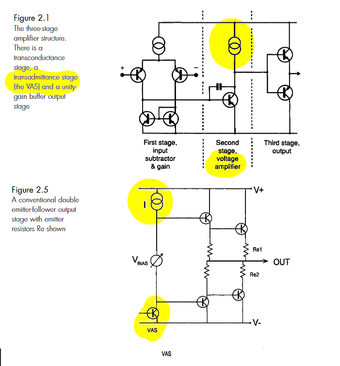
Douglas Self uses the term voltage amplifier stage (VAS) otherwise known as a "transadmittance" stage using this current source on the collector.
[![enter image description here][1]][1]
†( as Mr. Self calls it) [1]: https://i.sstatic.net/idpWs.png
Any comment on R11 and how to select R17 value?
R11 only serves to share dumping P=VI, DC power with Q5. If I ≈ 6mA then R11 dissipates 132 mW and reduces Q5 to some(?) value below 200mW.
R17 controls all the collector current of Q6 from R13+R14 (2 to 2.5mA) and leaves a small amount for both base currents I would choose R17 = 10% of R13+14 which affects CC value as much hFE variations of 300%. It's not critical. So I would pick 2K +/-1K. The high open loop gain is DC stabilized by the negative feedback R28 andvia R16. The lower R17 value reduces the current mirrors slightly and thus runs Q5 & Q7 a bit cooler.

