Commonmark migration
Source Link

After introducing the two-stages op-amp and frequency compensation for this circuit, during lecture the Professor asked us to find as an exercise a possible polarization of the following circuit:

[![enter image description here][1]][1]enter image description here
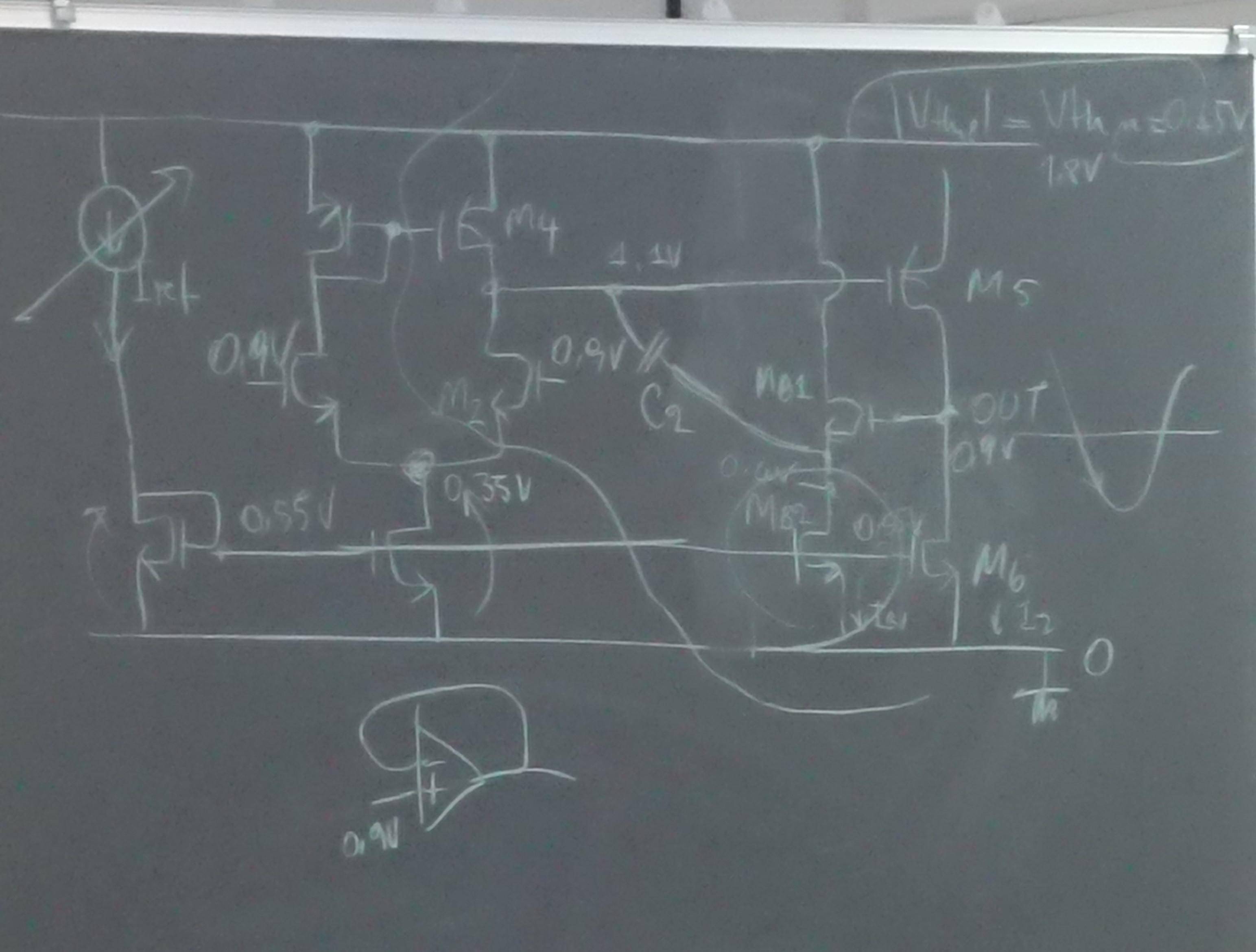
in which by hypothesis Vdd=1.8V and the input dc common mode is 0.9V. While solving together this exercise, the Professor said that, in order to use this circuit in the unity gain buffer configuration, the output dc voltage must be set equal to 0.9V. In this way the input dc common mode coincides with the output dc voltage, as required by the unity gain buffer configuration.

Question: why do I have to "artificially" impose that the output dc voltage is equal to the input dc common mode in order to have unity gain buffer configuration? Is not the negative feedback which imposes Vout=Vin? [1]: https://i.sstatic.net/pm8Te.jpg

After introducing the two-stages op-amp and frequency compensation for this circuit, during lecture the Professor asked us to find as an exercise a possible polarization of the following circuit:

[![enter image description here][1]][1]

in which by hypothesis Vdd=1.8V and the input dc common mode is 0.9V. While solving together this exercise, the Professor said that, in order to use this circuit in the unity gain buffer configuration, the output dc voltage must be set equal to 0.9V. In this way the input dc common mode coincides with the output dc voltage, as required by the unity gain buffer configuration.

Question: why do I have to "artificially" impose that the output dc voltage is equal to the input dc common mode in order to have unity gain buffer configuration? Is not the negative feedback which imposes Vout=Vin? [1]: https://i.sstatic.net/pm8Te.jpg

After introducing the two-stages op-amp and frequency compensation for this circuit, during lecture the Professor asked us to find as an exercise a possible polarization of the following circuit:

enter image description here

in which by hypothesis Vdd=1.8V and the input dc common mode is 0.9V. While solving together this exercise, the Professor said that, in order to use this circuit in the unity gain buffer configuration, the output dc voltage must be set equal to 0.9V. In this way the input dc common mode coincides with the output dc voltage, as required by the unity gain buffer configuration.

Question: why do I have to "artificially" impose that the output dc voltage is equal to the input dc common mode in order to have unity gain buffer configuration? Is not the negative feedback which imposes Vout=Vin?

Source Link
Stefanino
  • 616
  • 5
  • 17

Question about the common mode

After introducing the two-stages op-amp and frequency compensation for this circuit, during lecture the Professor asked us to find as an exercise a possible polarization of the following circuit:

[![enter image description here][1]][1]

in which by hypothesis Vdd=1.8V and the input dc common mode is 0.9V. While solving together this exercise, the Professor said that, in order to use this circuit in the unity gain buffer configuration, the output dc voltage must be set equal to 0.9V. In this way the input dc common mode coincides with the output dc voltage, as required by the unity gain buffer configuration.

Question: why do I have to "artificially" impose that the output dc voltage is equal to the input dc common mode in order to have unity gain buffer configuration? Is not the negative feedback which imposes Vout=Vin? [1]: https://i.sstatic.net/pm8Te.jpg