English and punctuation
Source Link
winny
  • 16.8k
  • 6
  • 50
  • 71

I am referring to datasheet of LM3743 block diagram in Pg no.page 5.

Datasheet

The EA and PWM Comp is in leading edge modulator configuration. According to my understanding SR latch which comes after PWM Comp must be R (Reset) must be triggered by Clock and S (Set) must be output of PWM Comp.

Example below gives better understanding.

Example

Which determines duty cycle on time of Vx or off time in figure b  ? What are these configurations called in industry (keyword)  ?

Should IL (Inductorinductor current) should have raise during off time of Vx (Figure b) or fall from peak value during off time Vx (Figure b)?

Further latchLatch output Vx (Figure b) is given to gate driver high side and low side.

I am referring to datasheet of LM3743 block diagram in Pg no. 5

Datasheet

The EA and PWM Comp is in leading edge modulator configuration. According to my understanding SR latch which comes after PWM Comp must be R (Reset) must be triggered by Clock and S (Set) must be output of PWM Comp.

Example below gives better understanding.

Example

Which determines duty cycle on time of Vx or off time in figure b  ? What are these configurations called in industry (keyword)  ?

Should IL (Inductor current) should have raise during off time of Vx (Figure b) or fall from peak value during off time Vx (Figure b)

Further latch output Vx (Figure b) is given to gate driver high side and low side.
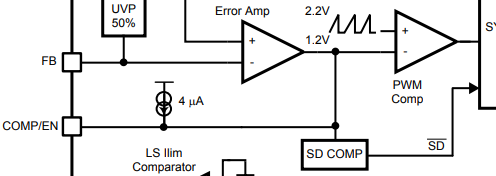
I am referring to datasheet of LM3743 block diagram in page 5.

Datasheet

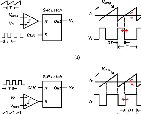
The EA and PWM Comp is in leading edge modulator configuration. According to my understanding SR latch which comes after PWM Comp must be R (Reset) must be triggered by Clock and S (Set) must be output of PWM Comp.

Example below gives better understanding.

Example

Which determines duty cycle on time of Vx or off time in figure b? What are these configurations called in industry (keyword)?

Should IL (inductor current) raise during off time of Vx (Figure b) or fall from peak value during off time Vx (Figure b)?

Latch output Vx (Figure b) is given to gate driver high side and low side.
Source Link
Pai
  • 305
  • 2
  • 15

PWM modulator in voltage mode buck converter

I am referring to datasheet of LM3743 block diagram in Pg no. 5

Datasheet

The EA and PWM Comp is in leading edge modulator configuration. According to my understanding SR latch which comes after PWM Comp must be R (Reset) must be triggered by Clock and S (Set) must be output of PWM Comp.

Example below gives better understanding.

Example

Which determines duty cycle on time of Vx or off time in figure b ? What are these configurations called in industry (keyword) ?

Should IL (Inductor current) should have raise during off time of Vx (Figure b) or fall from peak value during off time Vx (Figure b)

Further latch output Vx (Figure b) is given to gate driver high side and low side.