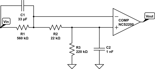
I havefound the following data slicer circuit:

simulate this circuit – Schematic created using CircuitLab
The input is a simple NRZ (PAM-2) signal between "Vhigh" and "Vlow" (=around 0V) where each bit has a length "Tbit". Due to bandwidth limitation, the input is also not a perfect square pulse but can be modeled as being filtered with a simple first-order lowpass with cutoff "fc".
The bit pattern is not givenI can't wrap my head around why exactly the author or this circuit came up with the idea of adding R1+C1 (it is not necessarily a self clocking codeand R3) but. I couldcannot find a single where adding R1+C1 would not make certain assumptionsthings worse (e.g. max. number of consecutive zeros or onesafter all, it's a highpass/differentiator). Similarly, I neigher see the purpose for R3, nore can I find a case where it would be helpful.
I do know how to roughly massageIn LTspice, the right values "qualitatively"circuit works best if I kick out R1,C1 and R3 and make R2*C3 = 5/Tbit (=spice monkeyingas suggested in https://www.maximintegrated.com/en/design/technical-documents/app-notes/3/3671.html).
But what is the proper procedure to quantitatively find these values based on Tbit, fc, Vhigh/Vlow and assumptions on bit pattern?
Based on the values seen on the schematic, can we determine for which kind of signal this circuit has been designed for?
Does the hystersis of the comparator (the NCS2200 has a typical internal hysteresis of 8mV) have anything to do with the design decisions?
EDIT: This is a possible example signal:
 But I don't want to remove just just because I don't understand it...
InEDIT: Maybe this case, Vlow=0, Vhigh=4mVwas a "hard" question so I changed it to merely (butunderstand what this can always be higher), Tbit=50us, and fc=3thing is doing.18kHz. Clearly the output should be 0,0,1,0,1,1,0,1,0,1,1,0,1 (1 being the voltage rail of the comparator).
