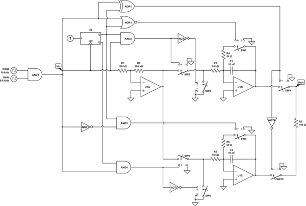
minor cleanup for switch orientation
Source Link
Reinderien
  • 3.3k
  • 17
  • 33

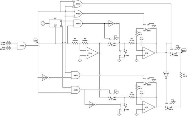
For theory-learning purposes I wanted to see if I could design a DAC that converts a 10 kHz PWM duty cycle to an analog waveform in a sample-and-hold manner with leap-frogging capacitive integrators, so that the charge-discharge ripple seen in a simple RC DAC is not present. My first stab at it uses ideal switching to focus on the basics:
schematicschematic

simulate this circuitsimulate this circuit – Schematic created using CircuitLab

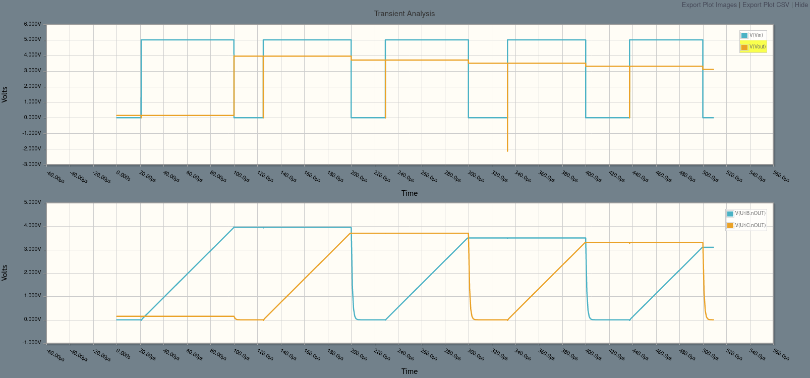
For each integrator, there are basically four segments: discharge, charge, output, output. This more or less works:

transient

The two PWM inputs are to simulate a single input whose duty cycle is changing.

Problems I see:

  • There are some glitches around the logic transitions
  • Any mismatch in the time constants between the two integrators is going to create square ripple cycle to cycle
  • This seems more complicated than it needs to be
  • I needed R7 because one of the glitches looks like temporary contention between the two integrator outputs
  • In its current configuration, the integrators require the inverter of U1A, which in turn would require a negative voltage supply I'd prefer not to need
  • Though this should reduce ripple when compared to a simple RC DAC, the square transitions from level to level will create aliasing components in the spectrum at multiples of the PWM frequency, and these components might themselves require an antialiasing RC stage anyway to get rid of

Questions:

  • Is this at all a standard approach to DAC design? If so, what's it called?
  • If implemented correctly, what advantages and disadvantages are there to this approach when compared to simple RC other than complexity?
  • For the switches, would single MOSFET pass-gates suffice?
  • How can this be simplified?
  • How best to reduce the glitches?
  • Can R7 be dropped?

For theory-learning purposes I wanted to see if I could design a DAC that converts a 10 kHz PWM duty cycle to an analog waveform in a sample-and-hold manner with leap-frogging capacitive integrators, so that the charge-discharge ripple seen in a simple RC DAC is not present. My first stab at it uses ideal switching to focus on the basics:

schematic

simulate this circuit – Schematic created using CircuitLab

For each integrator, there are basically four segments: discharge, charge, output, output. This more or less works:

transient

The two PWM inputs are to simulate a single input whose duty cycle is changing.

Problems I see:

  • There are some glitches around the logic transitions
  • Any mismatch in the time constants between the two integrators is going to create square ripple cycle to cycle
  • This seems more complicated than it needs to be
  • I needed R7 because one of the glitches looks like temporary contention between the two integrator outputs
  • In its current configuration, the integrators require the inverter of U1A, which in turn would require a negative voltage supply I'd prefer not to need
  • Though this should reduce ripple when compared to a simple RC DAC, the square transitions from level to level will create aliasing components in the spectrum at multiples of the PWM frequency, and these components might themselves require an antialiasing RC stage anyway to get rid of

Questions:

  • Is this at all a standard approach to DAC design? If so, what's it called?
  • If implemented correctly, what advantages and disadvantages are there to this approach when compared to simple RC other than complexity?
  • For the switches, would single MOSFET pass-gates suffice?
  • How can this be simplified?
  • How best to reduce the glitches?
  • Can R7 be dropped?
Source Link
Reinderien
  • 3.3k
  • 17
  • 33

Low-ripple sample-and-hold PWM DAC

For theory-learning purposes I wanted to see if I could design a DAC that converts a 10 kHz PWM duty cycle to an analog waveform in a sample-and-hold manner with leap-frogging capacitive integrators, so that the charge-discharge ripple seen in a simple RC DAC is not present. My first stab at it uses ideal switching to focus on the basics:

schematic

simulate this circuit – Schematic created using CircuitLab

For each integrator, there are basically four segments: discharge, charge, output, output. This more or less works:

transient

The two PWM inputs are to simulate a single input whose duty cycle is changing.

Problems I see:

  • There are some glitches around the logic transitions
  • Any mismatch in the time constants between the two integrators is going to create square ripple cycle to cycle
  • This seems more complicated than it needs to be
  • I needed R7 because one of the glitches looks like temporary contention between the two integrator outputs
  • In its current configuration, the integrators require the inverter of U1A, which in turn would require a negative voltage supply I'd prefer not to need
  • Though this should reduce ripple when compared to a simple RC DAC, the square transitions from level to level will create aliasing components in the spectrum at multiples of the PWM frequency, and these components might themselves require an antialiasing RC stage anyway to get rid of

Questions:

  • Is this at all a standard approach to DAC design? If so, what's it called?
  • If implemented correctly, what advantages and disadvantages are there to this approach when compared to simple RC other than complexity?
  • For the switches, would single MOSFET pass-gates suffice?
  • How can this be simplified?
  • How best to reduce the glitches?
  • Can R7 be dropped?