Clarification.
Source Link
TonyM
  • 23.8k
  • 4
  • 40
  • 65

(I'll stick with DFFs and use FPGAs as the example...)

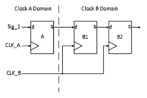
When a DFF in clock domain B (cdB) is driven by a DFF in clock domain A (cdA), the cdB DFF can go metastable if its setup/hold times are not met i.e. the input changes when the cdB clock is changing. You know that already.

enter image description here

Internally, the circuit of each DFF has a very high gain and uses positive feedback. It doesn't stay perfectly balanced in the metastable state and- it quickly heads towards one of the rails and, into a stable 0 or 1.

Let's now consider cdB DFF_B1 driving a combinatorial circuit that goes into further DFFs. While cdB DFF_B1 output isn't outputting a true 0/1 voltage, the driven combinatorial circuits can also produce invalid or incorrect outputs. When cdB DFF_B1 recovers sufficiently, that combinatorial circuit can correct itself but that circuit's output DFFs may be clocked before it does. The likelihood of that depends on the exact circuit, parts used and the clock frequency.

There are two functions of the second DFF (DFF_B2) in a 2-stage domain input shift register:

(1) When DFF_B1 is clocked and goes from stable into metastable, DFF_B2 will have a whole clock period before it latches in the was-metastable value. In that time, the DFF_B1 output will have headed towards a supply rail and partly/entirely resolved itself. DFF_B2 has a better input voltage to sample and itself resolve.

(2) The DFF_B1 metastable voltage reaches only one further input: DFF_B2's. It doesn't drive any combinatorial logic that can cause the problem detailed above.

So the cdB DFF_B2 is necessary unless the final circuit is simple/slow-clocked enough. I have seen a circuit pass aerospace inspection with only one domain input DFF because it had simple gating and ran at 1 MHz. (It was only found once in the field, otherwise it would have been given two DFFs.)

It's also one of the factors I use when selecting the lowest clock frequency I can be sure of for a digital circuit.

For FPGAs, the DFF recovery time is usually specified in part reliability specifications (haven't checked all manfs but Xilinx/Altera do).

Last time I checked recent families, it was sub-1 ns. This is much shorter than a clock period at the part's maximum clock frequencies (see datasheets).

(I'll stick with DFFs and use FPGAs as the example...)

When a DFF in clock domain B (cdB) is driven by a DFF in clock domain A (cdA), the cdB DFF can go metastable if its setup/hold times are not met i.e. the input changes when the cdB clock is changing. You know that already.

enter image description here

Internally, the circuit of each DFF has a very high gain and uses positive feedback. It doesn't stay balanced in the metastable state and heads towards one of the rails and into a stable 0 or 1.

Let's now consider cdB DFF_B1 driving a combinatorial circuit that goes into further DFFs. While cdB DFF_B1 output isn't outputting a true 0/1 voltage, the driven combinatorial circuits can also produce invalid or incorrect outputs. When cdB DFF_B1 recovers sufficiently, that combinatorial circuit can correct itself but that circuit's output DFFs may be clocked before it does. The likelihood of that depends on the exact circuit, parts used and the clock frequency.

There are two functions of the second DFF (DFF_B2) in a 2-stage domain input shift register:

(1) When DFF_B1 is clocked and goes from stable into metastable, DFF_B2 will have a whole clock period before it latches in the was-metastable value. In that time, the DFF_B1 output will have headed towards a supply rail and partly/entirely resolved itself. DFF_B2 has a better input voltage to sample and itself resolve.

(2) The DFF_B1 metastable voltage reaches only one further input: DFF_B2's. It doesn't drive any combinatorial logic that can cause the problem detailed above.

So the cdB DFF_B2 is necessary unless the final circuit is simple/slow-clocked enough. I have seen a circuit pass aerospace inspection with only one domain input DFF because it had simple gating and ran at 1 MHz. (It was only found once in the field, otherwise it would have been given two DFFs.)

It's also one of the factors I use when selecting the lowest clock frequency I can be sure of for a digital circuit.

For FPGAs, the DFF recovery time is usually specified in part reliability specifications (haven't checked all manfs but Xilinx/Altera do).

Last time I checked recent families, it was sub-1 ns. This is much shorter than a clock period at the part's maximum clock frequencies (see datasheets).

(I'll stick with DFFs and use FPGAs as the example...)

When a DFF in clock domain B (cdB) is driven by a DFF in clock domain A (cdA), the cdB DFF can go metastable if its setup/hold times are not met i.e. the input changes when the cdB clock is changing. You know that already.

enter image description here

Internally, the circuit of each DFF has a very high gain and uses positive feedback. It doesn't stay perfectly balanced in the metastable state - it quickly heads towards one of the rails, into a stable 0 or 1.

Let's now consider cdB DFF_B1 driving a combinatorial circuit that goes into further DFFs. While cdB DFF_B1 output isn't outputting a true 0/1 voltage, the driven combinatorial circuits can also produce invalid or incorrect outputs. When cdB DFF_B1 recovers sufficiently, that combinatorial circuit can correct itself but that circuit's output DFFs may be clocked before it does. The likelihood of that depends on the exact circuit, parts used and the clock frequency.

There are two functions of the second DFF (DFF_B2) in a 2-stage domain input shift register:

(1) When DFF_B1 is clocked and goes from stable into metastable, DFF_B2 will have a whole clock period before it latches in the was-metastable value. In that time, the DFF_B1 output will have headed towards a supply rail and partly/entirely resolved itself. DFF_B2 has a better input voltage to sample and itself resolve.

(2) The DFF_B1 metastable voltage reaches only one further input: DFF_B2's. It doesn't drive any combinatorial logic that can cause the problem detailed above.

So the cdB DFF_B2 is necessary unless the final circuit is simple/slow-clocked enough. I have seen a circuit pass aerospace inspection with only one domain input DFF because it had simple gating and ran at 1 MHz. (It was only found once in the field, otherwise it would have been given two DFFs.)

It's also one of the factors I use when selecting the lowest clock frequency I can be sure of for a digital circuit.

For FPGAs, the DFF recovery time is usually specified in part reliability specifications (haven't checked all manfs but Xilinx/Altera do).

Last time I checked recent families, it was sub-1 ns. This is much shorter than a clock period at the part's maximum clock frequencies (see datasheets).

Clarifications.
Source Link
TonyM
  • 23.8k
  • 4
  • 40
  • 65

(I'll stick with DFFs and use FPGAs as the example...)

When a DFF in clock domain 2B (cd2cdB) is driven by a DFF in clock domain 1A (cd1cdA), the cd2cdB DFF can go metastable if its setup/hold times are not met i.e. the input changes when the cd2cdB clock is changing. You know that already.

The DFFenter image description here

Internally, the circuit of each DFF has a very high gain and uses positive feedback. It doesn't stay balanced in the metastable state and heads towards one of the rails and into a stable 0 or 1.

Let's now examine cd2 DFFconsider cdB DFF_B1 driving a combinatorial circuit that goes into further DFFs. While cd2 DFFcdB DFF_B1 output isn't outputting a true 0/1 voltage, the driven combinatorial circuits can also produce invalid or incorrect outputs. When cd2 DFFcdB DFF_B1 recovers sufficiently, that combinatorial circuit can correct itself but its ownthat circuit's output DFFs may be clocked before it does. The likelihood of that depends on the exact circuit and, parts used and itsthe clock frequency.

There are two functions of the second DFF (DFF_B2) in a 2-stage domain input shift register:

(1) When DFF1DFF_B1 is clocked and goes from stable into metastable, DFF2DFF_B2 will have a whole clock period before it latches in the was-metastable value. In that time, DFF1'sthe DFF_B1 output will have headed towards a supply rail and partly/entirely resolved itself. DFF2DFF_B2 has a better input voltage to sample and itself resolve.

(2) The DFF1DFF_B1 metastable voltage reaches only one further input: DFF2'sDFF_B2's. It doesn't drive any combinatorial logic andthat can cause the problem detailed above.

So the cd2 DFF2cdB DFF_B2 is necessary unless the final circuit is simple/slow-clocked enough. I have seen a circuit pass aerospace inspection with only one domain input DFF because it had simple gating and ran at 1 MHz. (It was only found once in the field, otherwise it would have been given two DFFs.)

It's also one of the factors I use when selecting the lowest clock frequency I can be sure of for a digital circuit.

For FPGAs, the DFF recovery time is usually specified in part reliability specifications (haven't checked all manfs but Xilinx/Altera do).

Last time I checked recent families, it was sub-1 ns. This is much shorter than a clock period at the part's maximum clock frequencies (see datasheets).

(I'll stick with DFFs and use FPGAs as the example...)

When a DFF in clock domain 2 (cd2) is driven by a DFF in clock domain 1 (cd1), the cd2 DFF can go metastable if its setup/hold times are not met i.e. the input changes when the cd2 clock is changing. You know that already.

The DFF circuit has a very gain and uses positive feedback. It doesn't stay balanced in the metastable state and heads towards one of the rails and into a stable 0 or 1.

Let's now examine cd2 DFF driving a combinatorial circuit that goes into further DFFs. While cd2 DFF output isn't outputting a true 0/1 voltage, the driven combinatorial circuits can also produce invalid or incorrect outputs. When cd2 DFF recovers sufficiently, that combinatorial circuit can correct itself but its own output DFFs may be clocked before it does. The likelihood of that depends on the exact circuit and parts used and its clock frequency.

There are two functions of the second DFF in a 2-stage domain input shift register:

(1) When DFF1 is clocked and goes from stable into metastable, DFF2 will have a whole clock period before it latches in the was-metastable value. In that time, DFF1's output will have headed towards a supply rail and partly/entirely resolved itself. DFF2 has a better input voltage to sample and itself resolve.

(2) The DFF1 metastable voltage reaches only one further input: DFF2's. It doesn't drive any combinatorial logic and cause the problem detailed above.

So the cd2 DFF2 is necessary unless the final circuit is simple/slow-clocked enough. I have seen a circuit pass aerospace inspection with only one domain input DFF because it had simple gating and ran at 1 MHz. (It was in the field otherwise it would have been given two DFFs.)

It's also one of the factors I use when selecting the lowest clock frequency I can be sure of for a digital circuit.

For FPGAs, the DFF recovery time is usually specified in part reliability specifications (haven't checked all manfs but Xilinx/Altera do).

Last time I checked recent families, it was sub-1 ns. This is much shorter than a clock period at the part's maximum clock frequencies (see datasheets).

(I'll stick with DFFs and use FPGAs as the example...)

When a DFF in clock domain B (cdB) is driven by a DFF in clock domain A (cdA), the cdB DFF can go metastable if its setup/hold times are not met i.e. the input changes when the cdB clock is changing. You know that already.

enter image description here

Internally, the circuit of each DFF has a very high gain and uses positive feedback. It doesn't stay balanced in the metastable state and heads towards one of the rails and into a stable 0 or 1.

Let's now consider cdB DFF_B1 driving a combinatorial circuit that goes into further DFFs. While cdB DFF_B1 output isn't outputting a true 0/1 voltage, the driven combinatorial circuits can also produce invalid or incorrect outputs. When cdB DFF_B1 recovers sufficiently, that combinatorial circuit can correct itself but that circuit's output DFFs may be clocked before it does. The likelihood of that depends on the exact circuit, parts used and the clock frequency.

There are two functions of the second DFF (DFF_B2) in a 2-stage domain input shift register:

(1) When DFF_B1 is clocked and goes from stable into metastable, DFF_B2 will have a whole clock period before it latches in the was-metastable value. In that time, the DFF_B1 output will have headed towards a supply rail and partly/entirely resolved itself. DFF_B2 has a better input voltage to sample and itself resolve.

(2) The DFF_B1 metastable voltage reaches only one further input: DFF_B2's. It doesn't drive any combinatorial logic that can cause the problem detailed above.

So the cdB DFF_B2 is necessary unless the final circuit is simple/slow-clocked enough. I have seen a circuit pass aerospace inspection with only one domain input DFF because it had simple gating and ran at 1 MHz. (It was only found once in the field, otherwise it would have been given two DFFs.)

It's also one of the factors I use when selecting the lowest clock frequency I can be sure of for a digital circuit.

For FPGAs, the DFF recovery time is usually specified in part reliability specifications (haven't checked all manfs but Xilinx/Altera do).

Last time I checked recent families, it was sub-1 ns. This is much shorter than a clock period at the part's maximum clock frequencies (see datasheets).

Source Link
TonyM
  • 23.8k
  • 4
  • 40
  • 65

(I'll stick with DFFs and use FPGAs as the example...)

When a DFF in clock domain 2 (cd2) is driven by a DFF in clock domain 1 (cd1), the cd2 DFF can go metastable if its setup/hold times are not met i.e. the input changes when the cd2 clock is changing. You know that already.

The DFF circuit has a very gain and uses positive feedback. It doesn't stay balanced in the metastable state and heads towards one of the rails and into a stable 0 or 1.

Let's now examine cd2 DFF driving a combinatorial circuit that goes into further DFFs. While cd2 DFF output isn't outputting a true 0/1 voltage, the driven combinatorial circuits can also produce invalid or incorrect outputs. When cd2 DFF recovers sufficiently, that combinatorial circuit can correct itself but its own output DFFs may be clocked before it does. The likelihood of that depends on the exact circuit and parts used and its clock frequency.

There are two functions of the second DFF in a 2-stage domain input shift register:

(1) When DFF1 is clocked and goes from stable into metastable, DFF2 will have a whole clock period before it latches in the was-metastable value. In that time, DFF1's output will have headed towards a supply rail and partly/entirely resolved itself. DFF2 has a better input voltage to sample and itself resolve.

(2) The DFF1 metastable voltage reaches only one further input: DFF2's. It doesn't drive any combinatorial logic and cause the problem detailed above.

So the cd2 DFF2 is necessary unless the final circuit is simple/slow-clocked enough. I have seen a circuit pass aerospace inspection with only one domain input DFF because it had simple gating and ran at 1 MHz. (It was in the field otherwise it would have been given two DFFs.)

It's also one of the factors I use when selecting the lowest clock frequency I can be sure of for a digital circuit.

For FPGAs, the DFF recovery time is usually specified in part reliability specifications (haven't checked all manfs but Xilinx/Altera do).

Last time I checked recent families, it was sub-1 ns. This is much shorter than a clock period at the part's maximum clock frequencies (see datasheets).