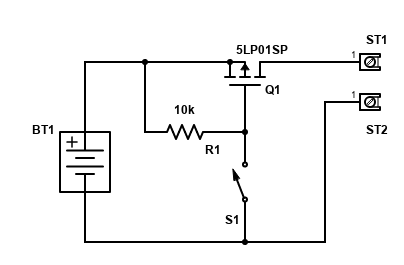
I have a fairly simple application:
Q1 is a P-Channel MOSFET. It had a flyback diode between drain and source (which is not illustrated here.)
Between ST1 and ST2 there is a 1k resistor to load the circuit by 5mA (BT provides 5V output.)
Unluckily, BT1 is providing negative voltage when it is turned off (-3V.)
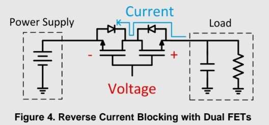
I came across with this circuit by TI:
I have some question about this, and I couldn't really find answers:
- What kind of MOSFETs are being used? (N or P channels?) I believe they should be P-channels, as their arrow is pointing out from them. However, in my diagram, the arrow is pointing towards the source while these are pointing towards the drain.
- Is this only a drawing difference? In other words, which one of these two would be my Q1? The left one or the right one? (I believe right one based on the flyback diode.)
- I can understand how this blocks reverse current when the gates are on GND. When they are opened up, I understand the right FET: current flows from source to drain (from left-to-right on the figure,) but what happens with the left FET? Why would current flow from drain to source in a P-FET?
Update
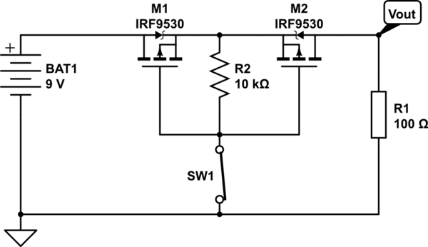
According to @nanofarad's suggestion, I've tried this circuit:
Although I don't yet have these FETs, so I used two 5LP01SP instead of them.
Please note, R1 is 1K to stay on the safe side.
Normally the powerbank provides a negative voltage on its output when turned off (-3V).
However with this circuit, there is only -0.8V on its output. I would say there is a 2V drop (not drop technically as the voltage is being increased, but I don't know how to express it)!
Why this drop is being introduced on negative voltage? Should not this circuit block reverese current, and therefore also voltage dropping?


