What's wrong with a breadboard?
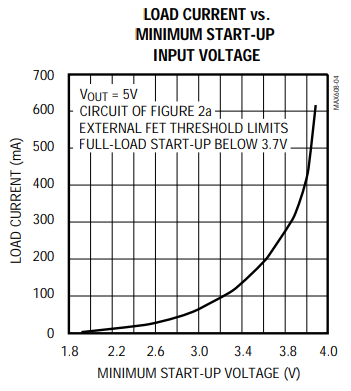
The current-sense resistor is important. If you don't have one to hand, it may be tempting to use Mehdi's video on how to create one using a wire, but when using a breadboard or perf board, you'll probably get undesirable results. I attempted to create a 50mΩ current-sense resistor as recommended in figure 2a, which should have allowed a 0.5A output current, but unfortunately adding a load above 150 mA caused the output voltage to collapse back to VIN. This problem with current limitingThis problem with current limiting not behaving as expected is probably due to using a breadboard/perf board.
Edit: Ok, so it turns out that the breadboard may not behaving as expected is probably duehave been the culprit for this problem; rather that the IC won't be able to usingprovide anything over about 20mA with a breadboard/perf board2V input.
Mostly for noise reduction, it seems.
"Bypass REF with a 0.1µF capacitor (C3)."
"high capacitance values may degrade line regulation."
I have noticed that using too higher capacitance value does indeed cause the output Maybe a bit trickier to behave strangelydo on a breadboard, since with PCB design you can create significantly shorter paths with less resistance.
Something else that's quite tricky to do with a prototype, since jumper wires have quite a lot of resistance.
"there is a resistance around 40 ohms between the OUT and GND pin. But I'm still not sure if it is really supposed to be that way; I couldn't find anything about this in the data sheet"
There is supposed to be no connection within the IC itself between OUT (2) and GND (7); one of my fried chips had a 9 ohms impedance, whereas the others displayed overload on the multimeter; totally open, it seems.
Edit: This is probably because OUT is actually the input power for the IC; a short indicates that too much voltage flowed into the OUT pin, causing them to short permanently. The only output pin from what I can tell is actually EXT, the FET gate driver.Also possibly of interest
~~From this, I assume that there should always be some kind of load; but what happens if not? The datasheet doesn't make that clear, but it does mention it twice... however, from my observations, the output signal appears to behave just fine when there is no load.~~From this, I assume that there should always be some kind of load; but what happens if not? The datasheet doesn't make that clear, but it does mention it twice... however, from my observations, the output signal appears to behave just fine when there is no load.
I actually used a FET with max 500mA on the prototype, but in hindsight, I had plenty of power FETs, so perhaps I should have used one of those. The input current will be quite high compared the output current, so maybe this is where some of my current problems came from. Maybe I'll swap that out for a nice hefty IRLB FET for my PCB.
"Bypass REF with a 0.1µF capacitor (C3)."
"high capacitance values may degrade line regulation."
I have noticed that using too higher capacitance value does indeed cause the output to behave strangely. But, not sure if this could lead to the chip being damaged.
Edit: AppendixOUT (2) and GND (7)
"there is a resistance around 40 ohms between the OUT and GND pin. But I'm still not sure if it is really supposed to be that way; I couldn't find anything about this in the data sheet"
There is supposed to be no connection within the IC itself between OUT (2) and GND (7); one of my fried chips had a 9 ohms impedance, whereas the others displayed overload on the multimeter; totally open, it seems.
Edit: This is probably because OUT is actually the input power for the IC; a short indicates that too much voltage flowed into the OUT pin, causing them to short permanently. The only output pin from what I can tell is actually EXT, the FET gate driver.
Edit 2: I actually ordered some more, so this'll be the first thing I test when they arrive. You know what, I suppose that it's possible it's supposed to shorted like that. We'll soon see.
Dead bug on ground plane

