Ok, so I made the same mistake as you! I even shorted OUT and GND (9 ohms) on one chip. I tried the MAX608 on a breadboard first before going to perf board prototype. I then built a perf board prototype too, and that behaved differently to the breadboard. Also, possibly of interest, I tried the TL499ACP (a chip designed for a similar purpose), and had even worse results on the breadboard.
"I think It is reasonable to try it first on a prototype board"
I thought so too. I since changed my mind when it comes to DCDC converters.
Anyway, five fried chips later, and hours wasted, I finally learned my lesson...
Lesson: As the others have recommended in the comments, don't prototype a DCDC converter on a breadboard or perf board; go straight to PCB design and follow the datasheet to the letter. Without a proper PCB design, you might get something resembling good enough, but eventually, it seems that the chip will fail and it'll probably behave nothing like the PCB version.
I also learned the hard way that this principle isn't limited to DCDC converters, and there are other types of design you can't practically breadboard, such as HDMI (and to a much less severe degree, VGA). RF also seems difficult on breadboard/perf board.
For the PCB design, here are my Cliff Notes from the MAX608 datasheet:
What's wrong with a breadboard?
"Due to high current levels and fast switching waveforms, which radiate noise, proper PC board layout is essential."
"Protect sensitive analog grounds by using a star ground configuration."
In other words, breadboard or perf board won't work. You can't get close at all to a PCB design by using prototypes, and while you might be able to do something like star ground on a prototype, the resistance from the jumper wires will cause behaviour very far from that of a ground plane.
"the MAX608 uses a sense resistor to control the peak inductor current"
"Connect the current-sense resistor between CS and AGND."
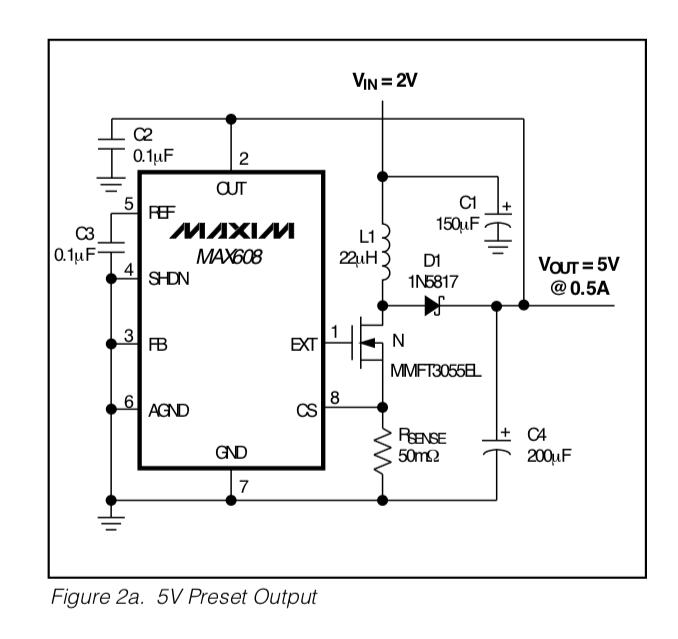
The current-sense resistor is important. If you don't have one to hand, it may be tempting to use Mehdi's video on how to create one using a wire, but when using a breadboard or perf board, you'll probably get undesirable results. I attempted to create a 50mΩ current-sense resistor as recommended in figure 2a, which should have allowed a 0.5A output current, but unfortunately adding a load above 150 mA caused the output voltage to collapse back to VIN. This problem with current limiting not behaving as expected is probably due to using a breadboard/perf board.
Edit: Ok, so it turns out that the breadboard may not have been the culprit for this problem; rather that the IC won't be able to provide anything over about 20mA with a 2V input.
"Bypass the IC with a 0.1µF ceramic capacitor (C2) placed as close as possible to the OUT and GND pins."
"Place input bypass capacitor C2 as close as possible to OUT and GND."
Mostly for noise reduction, it seems. Maybe a bit trickier to do on a breadboard, since with PCB design you can create significantly shorter paths with less resistance.
"If an external resistor divider is used (Figures 2 and 3), the trace from FB to the resistors must be extremely short."
Something else that's quite tricky to do with a prototype, since jumper wires have quite a lot of resistance.
Also possibly of interest
"If the inductor value is too low, the current will ramp up to a high level before the current-limit comparator can turn off the switch."
"smaller inductance values allow the coil current to ramp up to higher levels before the switch turns off, increasing the ripple at light loads."
I have actually seen this happen with a couple of the fried chips; even with the recommended 22µH inductor. So, if you see this happen, the chip may have gone bad. Be wary of what you're connecting to the output; even with the 5V setup you could see voltages as high as 15V, so consider adding a regulator after the output.
"Always connect OUT 2 to circuit output."*
"OUT must always be connected to the circuit output."
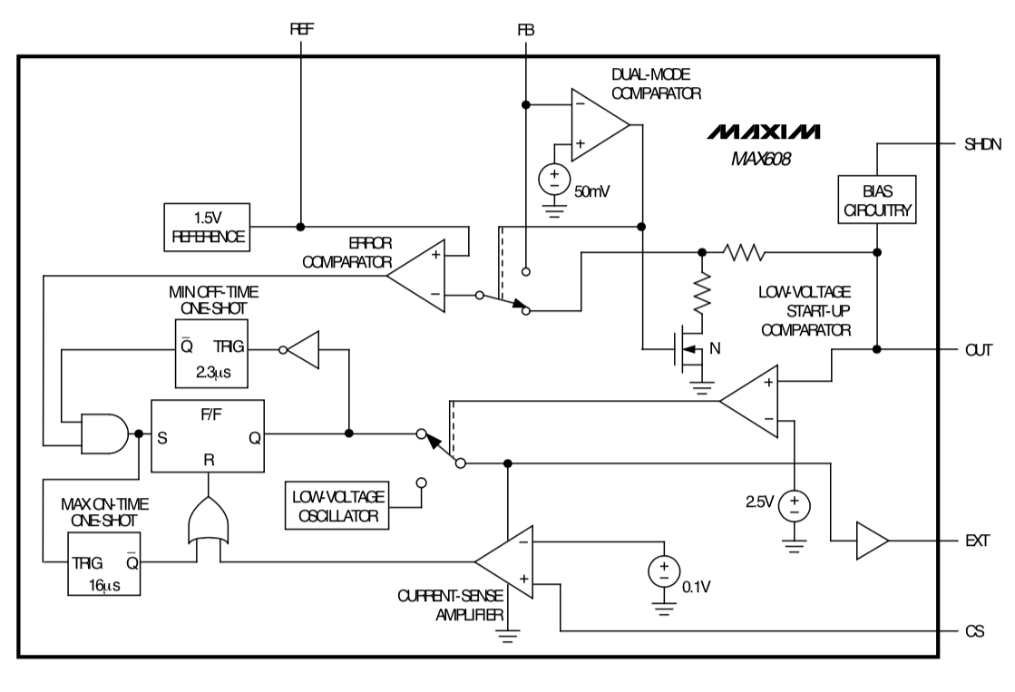
"The MAX608 operates in “bootstrapped” mode only (with the chip supply, OUT, connected to the DC-DC output)."
From this, I assume that there should always be some kind of load; but what happens if not? The datasheet doesn't make that clear, but it does mention it twice... however, from my observations, the output signal appears to behave just fine when there is no load.
Edit: So, the OUT pin is used for bootstrapped mode (to power the IC), which allows the chip to turn on in the first place; OUT is actually an input pin, which is confusing. But how will the IC turn on if EXT is low? The FET would be turned off. It's possible that either EXT or the gate on the FET will float, allowing the FET to turn on, powering the IC.
"Supply Voltage OUT to GND -0.3V, 17V"
Edit: The absolute maximum that OUT can take is 17V. If the IC is improperly configured or damaged, I have seen the output spike to around 15V, dangerously close to 17V. The datasheet doesn't say this, but perhaps a regulator or resistor might be useful on this pin.
"EXT, CS, REF, SHDN, FB to GND -0.3V, (VOUT + 0.3V)"
"GND to AGND 0.1V, -0.1V"
Edit: These are the absolute maximums. Any voltage applied to these pins will likely kill the chip, this is why connecting these to a ground plane is so important.
"Use an N-channel MOSFET power transistor with the MAX608."
I actually used a FET with max 500mA on the prototype, but in hindsight, I had plenty of power FETs, so perhaps I should have used one of those. The input current will be quite high compared the output current, so maybe this is where some of my current problems came from. Maybe I'll swap that out for a nice hefty IRLB FET for my PCB.
"Bypass REF with a 0.1µF capacitor (C3)."
"high capacitance values may degrade line regulation."
I have noticed that using too higher capacitance value does indeed cause the output to behave strangely. But, not sure if this could lead to the chip being damaged.
OUT (2) and GND (7)
"there is a resistance around 40 ohms between the OUT and GND pin. But I'm still not sure if it is really supposed to be that way; I couldn't find anything about this in the data sheet"
There is supposed to be no connection within the IC itself between OUT (2) and GND (7); one of my fried chips had a 9 ohms impedance, whereas the others displayed overload on the multimeter; totally open, it seems.
Edit: This is probably because OUT is actually the input power for the IC; a short indicates that too much voltage flowed into the OUT pin, causing them to short permanently. The only output pin from what I can tell is actually EXT, the FET gate driver.
Edit 2: I actually ordered some more, so this'll be the first thing I test when they arrive. You know what, I suppose that it's possible it's supposed to shorted like that. We'll soon see.
Dead bug on ground plane
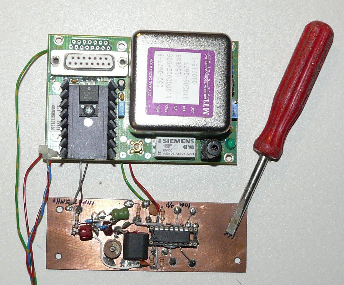
Edit: That said, if you do want to make a prototype with the MAX608 before doing a PCB run... Kuba's suggestion of using dead bug on ground plane led me to an interesting RF community discussion. The full images were password protected, so I thought resurfacing them as an answer might help someone. It seems that capacitance would be a design consideration with this approach.

Load current limitations
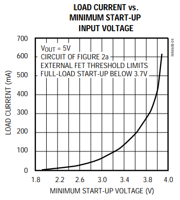
Edit: Not really related to your question, and I'll turn this into a new question, but I was also wondering why higher load currents (well within the advertised 1.5A limit) cause the chip to shut down. Turns out there's a minimum start-up voltage which depends on the load current. Very important to consider: e.g. a 2V supply/input on the MAX608 (5V output configuration) cannot power much beyond what looks like ~20mA.
Edit: I turned this into a new question...
Can a 3.3V peak 170mA device be reliably powered from only 2.5V?
