added 7 characters in body
Source Link
user4574
  • 12.5k
  • 18
  • 33

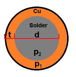
You can approximately estimate the resistance of a filled via by calculating the parallel resistance of a conductive cylinder (made of solder) and a conductive hollow cylinder (made of copper).

$$ R_{cu} = \frac{4*l*p_1}{\pi ((d+2t)^2 - d^2)} $$

$$ R_s = \frac{4*l*p_2}{\pi d^2 } $$

$$ R_{via} = \frac{R_{cu} * R_s}{R_{cu} + R_s} $$

enter image description here

  • t is the copper plating thickness in meters.
  • d is the via finished hole diameter in meters.
  • p1 is the resistivity of the copper plating Ω-m.
  • p2 is the resistivity of the solder fill in Ω-m.
  • l is the via length in meters.
  • Rcu is the copper resistance.
  • Rs is the solder resistance.
  • Rvia is the total resistance of the filled via.

Example1:
10 mil0.33mm finished hole diameter via with 1oz copper plating on a 1.6mm thick board filled with SnAgCu lead free solder.

$$ R_{cu} = \frac{4*1.6mm*17.4 nΩm}{\pi ((254um+2*35um)^2 - (254um)^2)} = 0.855mΩ$$$$ R_{cu} = \frac{4*1.6mm*17.4 nΩm}{\pi ((330um+2*35um)^2 - (330um)^2)} = 0.694mΩ$$

$$ R_s = \frac{4*1.6mm*120nΩm}{\pi (254um)^2 } = 3.78mΩ$$$$ R_s = \frac{4*1.6mm*120nΩm}{\pi (330um)^2 } = 2.24mΩ$$

$$ R_{via} = \frac{1.87mΩ * 3.78mΩ}{1.87mΩ + 3.78mΩ} = 0.697mΩ$$$$ R_{via} = \frac{1.87mΩ * 3.78mΩ}{1.87mΩ + 3.78mΩ} = 0.529mΩ$$

So, the filled via is about 82%76% the resistance of the unfilled one.

Example2:

20 mil1mm finished hole diameter via with 1oz copper plating on a 1.6mm thick board filled with SnAgCu lead free solder.

$$ R_{cu} = \frac{4*1.6mm*17.4 nΩm}{\pi ((508um+2*35um)^2 - (508um)^2)} = 0.455mΩ$$$$ R_{cu} = \frac{4*1.6mm*17.4 nΩm}{\pi ((1mm+2*35um)^2 - (1mm)^2)} = 0.245mΩ$$

$$ R_s = \frac{4*1.6mm*120nΩm}{\pi (508um)^2 } = 0.455mΩ$$$$ R_s = \frac{4*1.6mm*120nΩm}{\pi (1mm)^2 } = 0.244mΩ$$

$$ R_{via} = \frac{1.87mΩ * 3.78mΩ}{1.87mΩ + 3.78mΩ} = 0.307mΩ$$$$ R_{via} = \frac{1.87mΩ * 3.78mΩ}{1.87mΩ + 3.78mΩ} = 0.122mΩ$$

So, the filled via is about 67%50% the resistance of the unfilled one.

Note that even though the cross section of the solder fill is much larger than the cross section of the copper, its only having a minor effect due to the fact that the resistivity of the solder is like 7X higher.

There are other fillers (conductive epoxies) that you can use besides solder that may give much better results. There are also companies like NetVia Group that can fill the holes with solid copper if you wish.

Lastly, the resistance of the copper part is decreasing linearly with the reciprocal of the via diameter, but the resistance of the filled part is decreasing with the square of the reciprocal of the diameter. So the fill will have a lot more effect when using larger holes.

The fact that you are using a 10mm trace points to the possibility that your board is carrying 100A or more. Having done many boards like that, I would advise using lots of vias in a grid to avoid concentrating too much current in one place when making layer transitions. In some cases, I used as many as 20 filled vias when going from an inner layer into the pins of a high-power component. Also using multiple layers of 3-oz copper helps.

You can approximately estimate the resistance of a filled via by calculating the parallel resistance of a conductive cylinder (made of solder) and a conductive hollow cylinder (made of copper).

$$ R_{cu} = \frac{4*l*p_1}{\pi ((d+2t)^2 - d^2)} $$

$$ R_s = \frac{4*l*p_2}{\pi d^2 } $$

$$ R_{via} = \frac{R_{cu} * R_s}{R_{cu} + R_s} $$

enter image description here

  • t is the copper plating thickness in meters.
  • d is the via finished hole diameter in meters.
  • p1 is the resistivity of the copper plating Ω-m.
  • p2 is the resistivity of the solder fill in Ω-m.
  • l is the via length in meters.
  • Rcu is the copper resistance.
  • Rs is the solder resistance.
  • Rvia is the total resistance of the filled via.

Example1:
10 mil finished hole diameter via with 1oz copper plating on a 1.6mm thick board filled with SnAgCu lead free solder.

$$ R_{cu} = \frac{4*1.6mm*17.4 nΩm}{\pi ((254um+2*35um)^2 - (254um)^2)} = 0.855mΩ$$

$$ R_s = \frac{4*1.6mm*120nΩm}{\pi (254um)^2 } = 3.78mΩ$$

$$ R_{via} = \frac{1.87mΩ * 3.78mΩ}{1.87mΩ + 3.78mΩ} = 0.697mΩ$$

So, the filled via is about 82% the resistance of the unfilled one.

Example2:

20 mil finished hole diameter via with 1oz copper plating on a 1.6mm thick board filled with SnAgCu lead free solder.

$$ R_{cu} = \frac{4*1.6mm*17.4 nΩm}{\pi ((508um+2*35um)^2 - (508um)^2)} = 0.455mΩ$$

$$ R_s = \frac{4*1.6mm*120nΩm}{\pi (508um)^2 } = 0.455mΩ$$

$$ R_{via} = \frac{1.87mΩ * 3.78mΩ}{1.87mΩ + 3.78mΩ} = 0.307mΩ$$

So, the filled via is about 67% the resistance of the unfilled one.

Note that even though the cross section of the solder fill is much larger than the cross section of the copper, its only having a minor effect due to the fact that the resistivity of the solder is like 7X higher.

There are other fillers (conductive epoxies) that you can use besides solder that may give much better results. There are also companies like NetVia Group that can fill the holes with solid copper if you wish.

Lastly, the resistance of the copper part is decreasing linearly with the reciprocal of the via diameter, but the resistance of the filled part is decreasing with the square of the reciprocal of the diameter. So the fill will have a lot more effect when using larger holes.

The fact that you are using a 10mm trace points to the possibility that your board is carrying 100A or more. Having done many boards like that, I would advise using lots of vias in a grid to avoid concentrating too much current in one place when making layer transitions. In some cases, I used as many as 20 filled vias when going from an inner layer into the pins of a high-power component. Also using multiple layers of 3-oz copper helps.

You can approximately estimate the resistance of a filled via by calculating the parallel resistance of a conductive cylinder (made of solder) and a conductive hollow cylinder (made of copper).

$$ R_{cu} = \frac{4*l*p_1}{\pi ((d+2t)^2 - d^2)} $$

$$ R_s = \frac{4*l*p_2}{\pi d^2 } $$

$$ R_{via} = \frac{R_{cu} * R_s}{R_{cu} + R_s} $$

enter image description here

  • t is the copper plating thickness in meters.
  • d is the via finished hole diameter in meters.
  • p1 is the resistivity of the copper plating Ω-m.
  • p2 is the resistivity of the solder fill in Ω-m.
  • l is the via length in meters.
  • Rcu is the copper resistance.
  • Rs is the solder resistance.
  • Rvia is the total resistance of the filled via.

Example1:
0.33mm finished hole diameter via with 1oz copper plating on a 1.6mm thick board filled with SnAgCu lead free solder.

$$ R_{cu} = \frac{4*1.6mm*17.4 nΩm}{\pi ((330um+2*35um)^2 - (330um)^2)} = 0.694mΩ$$

$$ R_s = \frac{4*1.6mm*120nΩm}{\pi (330um)^2 } = 2.24mΩ$$

$$ R_{via} = \frac{1.87mΩ * 3.78mΩ}{1.87mΩ + 3.78mΩ} = 0.529mΩ$$

So, the filled via is about 76% the resistance of the unfilled one.

Example2:

1mm finished hole diameter via with 1oz copper plating on a 1.6mm thick board filled with SnAgCu lead free solder.

$$ R_{cu} = \frac{4*1.6mm*17.4 nΩm}{\pi ((1mm+2*35um)^2 - (1mm)^2)} = 0.245mΩ$$

$$ R_s = \frac{4*1.6mm*120nΩm}{\pi (1mm)^2 } = 0.244mΩ$$

$$ R_{via} = \frac{1.87mΩ * 3.78mΩ}{1.87mΩ + 3.78mΩ} = 0.122mΩ$$

So, the filled via is about 50% the resistance of the unfilled one.

Note that even though the cross section of the solder fill is much larger than the cross section of the copper, its only having a minor effect due to the fact that the resistivity of the solder is like 7X higher.

There are other fillers (conductive epoxies) that you can use besides solder that may give much better results. There are also companies like NetVia Group that can fill the holes with solid copper if you wish.

Lastly, the resistance of the copper part is decreasing linearly with the reciprocal of the via diameter, but the resistance of the filled part is decreasing with the square of the reciprocal of the diameter. So the fill will have a lot more effect when using larger holes.

The fact that you are using a 10mm trace points to the possibility that your board is carrying 100A or more. Having done many boards like that, I would advise using lots of vias in a grid to avoid concentrating too much current in one place when making layer transitions. In some cases, I used as many as 20 filled vias when going from an inner layer into the pins of a high-power component. Also using multiple layers of 3-oz copper helps.

added 7 characters in body
Source Link
user4574
  • 12.5k
  • 18
  • 33

You can approximately estimate the resistance of a filled via by calculating the parallel resistance of a conductive cylinder (made of solder) and a conductive hollow cylinder (made of copper).

$$ R_{cu} = \frac{4*l*p_1}{\pi ((d+t)^2 - d^2)} $$$$ R_{cu} = \frac{4*l*p_1}{\pi ((d+2t)^2 - d^2)} $$

$$ R_s = \frac{4*l*p_2}{\pi d^2 } $$

$$ R_{via} = \frac{R_{cu} * R_s}{R_{cu} + R_s} $$

enter image description here

  • t is the copper plating thickness in meters.
  • d is the via finished hole diameter in meters.
  • p1 is the resistivity of the copper plating Ω-m.
  • p2 is the resistivity of the solder fill in Ω-m.
  • l is the via length in meters.
  • Rcu is the copper resistance.
  • Rs is the solder resistance.
  • Rvia is the total resistance of the filled via.

Example1:
10 mil finished hole diameter via with 1oz copper plating on a 1.6mm thick board filled with SnAgCu lead free solder.

$$ R_{cu} = \frac{4*1.6mm*17.4 nΩm}{\pi ((254um+35um)^2 - (254um)^2)} = 1.87mΩ$$$$ R_{cu} = \frac{4*1.6mm*17.4 nΩm}{\pi ((254um+2*35um)^2 - (254um)^2)} = 0.855mΩ$$

$$ R_s = \frac{4*1.6mm*120nΩm}{\pi (254um)^2 } = 3.78mΩ$$

$$ R_{via} = \frac{1.87mΩ * 3.78mΩ}{1.87mΩ + 3.78mΩ} = 1.24mΩ$$$$ R_{via} = \frac{1.87mΩ * 3.78mΩ}{1.87mΩ + 3.78mΩ} = 0.697mΩ$$

So, the filled via is about 2/382% the resistance of the unfilled one.

Example2:

20 mil finished hole diameter via with 1oz copper plating on a 1.6mm thick board filled with SnAgCu lead free solder.

$$ R_{cu} = \frac{4*1.6mm*17.4 nΩm}{\pi ((508um+35um)^2 - (508um)^2)} = 0.964mΩ$$$$ R_{cu} = \frac{4*1.6mm*17.4 nΩm}{\pi ((508um+2*35um)^2 - (508um)^2)} = 0.455mΩ$$

$$ R_s = \frac{4*1.6mm*120nΩm}{\pi (508um)^2 } = 0.947mΩ$$$$ R_s = \frac{4*1.6mm*120nΩm}{\pi (508um)^2 } = 0.455mΩ$$

$$ R_{via} = \frac{1.87mΩ * 3.78mΩ}{1.87mΩ + 3.78mΩ} = 0.477mΩ$$$$ R_{via} = \frac{1.87mΩ * 3.78mΩ}{1.87mΩ + 3.78mΩ} = 0.307mΩ$$

So, the filled via is about 1/267% the resistance of the unfilled one.

Note that even though the cross section of the solder fill is much larger than the cross section of the copper, its only having a minor effect due to the fact that the resistivity of the solder is like 7X higher.

There are other fillers (conductive epoxies) that you can use besides solder that may give much better results. There are also companies like NetVia Group that can fill the holes with solid copper if you wish.

Lastly, the resistance of the copper part is decreasing linearly with the reciprocal of the via diameter, but the resistance of the filled part is decreasing with the square of the reciprocal of the diameter. So the fill will have a lot more effect when using larger holes.

The fact that you are using a 10mm trace points to the possibility that your board is carrying 100A or more. Having done many boards like that, I would advise using lots of vias in a grid to avoid concentrating too much current in one place when making layer transitions. In some cases, I used as many as 20 filled vias when going from an inner layer into the pins of a high-power component. Also using multiple layers of 3-oz copper helps.

You can approximately estimate the resistance of a filled via by calculating the parallel resistance of a conductive cylinder (made of solder) and a conductive hollow cylinder (made of copper).

$$ R_{cu} = \frac{4*l*p_1}{\pi ((d+t)^2 - d^2)} $$

$$ R_s = \frac{4*l*p_2}{\pi d^2 } $$

$$ R_{via} = \frac{R_{cu} * R_s}{R_{cu} + R_s} $$

enter image description here

  • t is the copper plating thickness in meters.
  • d is the via finished hole diameter in meters.
  • p1 is the resistivity of the copper plating Ω-m.
  • p2 is the resistivity of the solder fill in Ω-m.
  • l is the via length in meters.
  • Rcu is the copper resistance.
  • Rs is the solder resistance.
  • Rvia is the total resistance of the filled via.

Example1:
10 mil finished hole diameter via with 1oz copper plating on a 1.6mm thick board filled with SnAgCu lead free solder.

$$ R_{cu} = \frac{4*1.6mm*17.4 nΩm}{\pi ((254um+35um)^2 - (254um)^2)} = 1.87mΩ$$

$$ R_s = \frac{4*1.6mm*120nΩm}{\pi (254um)^2 } = 3.78mΩ$$

$$ R_{via} = \frac{1.87mΩ * 3.78mΩ}{1.87mΩ + 3.78mΩ} = 1.24mΩ$$

So, the filled via is about 2/3 the resistance of the unfilled one.

Example2:

20 mil finished hole diameter via with 1oz copper plating on a 1.6mm thick board filled with SnAgCu lead free solder.

$$ R_{cu} = \frac{4*1.6mm*17.4 nΩm}{\pi ((508um+35um)^2 - (508um)^2)} = 0.964mΩ$$

$$ R_s = \frac{4*1.6mm*120nΩm}{\pi (508um)^2 } = 0.947mΩ$$

$$ R_{via} = \frac{1.87mΩ * 3.78mΩ}{1.87mΩ + 3.78mΩ} = 0.477mΩ$$

So, the filled via is about 1/2 the resistance of the unfilled one.

Note that even though the cross section of the solder fill is much larger than the cross section of the copper, its only having a minor effect due to the fact that the resistivity of the solder is like 7X higher.

There are other fillers (conductive epoxies) that you can use besides solder that may give much better results. There are also companies like NetVia Group that can fill the holes with solid copper if you wish.

Lastly, the resistance of the copper part is decreasing linearly with the reciprocal of the via diameter, but the resistance of the filled part is decreasing with the square of the reciprocal of the diameter. So the fill will have a lot more effect when using larger holes.

The fact that you are using a 10mm trace points to the possibility that your board is carrying 100A or more. Having done many boards like that, I would advise using lots of vias in a grid to avoid concentrating too much current in one place when making layer transitions. In some cases, I used as many as 20 filled vias when going from an inner layer into the pins of a high-power component. Also using multiple layers of 3-oz copper helps.

You can approximately estimate the resistance of a filled via by calculating the parallel resistance of a conductive cylinder (made of solder) and a conductive hollow cylinder (made of copper).

$$ R_{cu} = \frac{4*l*p_1}{\pi ((d+2t)^2 - d^2)} $$

$$ R_s = \frac{4*l*p_2}{\pi d^2 } $$

$$ R_{via} = \frac{R_{cu} * R_s}{R_{cu} + R_s} $$

enter image description here

  • t is the copper plating thickness in meters.
  • d is the via finished hole diameter in meters.
  • p1 is the resistivity of the copper plating Ω-m.
  • p2 is the resistivity of the solder fill in Ω-m.
  • l is the via length in meters.
  • Rcu is the copper resistance.
  • Rs is the solder resistance.
  • Rvia is the total resistance of the filled via.

Example1:
10 mil finished hole diameter via with 1oz copper plating on a 1.6mm thick board filled with SnAgCu lead free solder.

$$ R_{cu} = \frac{4*1.6mm*17.4 nΩm}{\pi ((254um+2*35um)^2 - (254um)^2)} = 0.855mΩ$$

$$ R_s = \frac{4*1.6mm*120nΩm}{\pi (254um)^2 } = 3.78mΩ$$

$$ R_{via} = \frac{1.87mΩ * 3.78mΩ}{1.87mΩ + 3.78mΩ} = 0.697mΩ$$

So, the filled via is about 82% the resistance of the unfilled one.

Example2:

20 mil finished hole diameter via with 1oz copper plating on a 1.6mm thick board filled with SnAgCu lead free solder.

$$ R_{cu} = \frac{4*1.6mm*17.4 nΩm}{\pi ((508um+2*35um)^2 - (508um)^2)} = 0.455mΩ$$

$$ R_s = \frac{4*1.6mm*120nΩm}{\pi (508um)^2 } = 0.455mΩ$$

$$ R_{via} = \frac{1.87mΩ * 3.78mΩ}{1.87mΩ + 3.78mΩ} = 0.307mΩ$$

So, the filled via is about 67% the resistance of the unfilled one.

Note that even though the cross section of the solder fill is much larger than the cross section of the copper, its only having a minor effect due to the fact that the resistivity of the solder is like 7X higher.

There are other fillers (conductive epoxies) that you can use besides solder that may give much better results. There are also companies like NetVia Group that can fill the holes with solid copper if you wish.

Lastly, the resistance of the copper part is decreasing linearly with the reciprocal of the via diameter, but the resistance of the filled part is decreasing with the square of the reciprocal of the diameter. So the fill will have a lot more effect when using larger holes.

The fact that you are using a 10mm trace points to the possibility that your board is carrying 100A or more. Having done many boards like that, I would advise using lots of vias in a grid to avoid concentrating too much current in one place when making layer transitions. In some cases, I used as many as 20 filled vias when going from an inner layer into the pins of a high-power component. Also using multiple layers of 3-oz copper helps.

added 36 characters in body
Source Link
user4574
  • 12.5k
  • 18
  • 33

You can conservativelyapproximately estimate the resistance of a filled via by calculating the parallel resistance of a conductive cylinder (made of solder) and a conductive hollow cylinder (made of copper).

$$ R_{cu} = \frac{4*l*p_1}{\pi ((d+t)^2 - d^2)} $$

$$ R_s = \frac{4*l*p_2}{\pi d^2 } $$

$$ R_{via} = \frac{R_{cu} * R_s}{R_{cu} + R_s} $$

enter image description here

  • t is the copper plating thickness in meters.
  • d is the via finished hole diameter in meters.
  • p1 is the resistivity of the copper plating Ω-m.
  • p2 is the resistivity of the solder fill in Ω-m.
  • l is the via length in meters.
  • Rcu is the copper resistance.
  • Rs is the solder resistance.
  • Rvia is the total resistance of the filled via.

Example1:
10 mil finished hole diameter via with 1oz copper plating on a 1.6mm thick board filled with SnAgCu lead free solder.

$$ R_{cu} = \frac{4*1.6mm*17.4 nΩm}{\pi ((254um+35um)^2 - (254um)^2)} = 1.87mΩ$$

$$ R_s = \frac{4*1.6mm*120nΩm}{\pi (254um)^2 } = 3.78mΩ$$

$$ R_{via} = \frac{1.87mΩ * 3.78mΩ}{1.87mΩ + 3.78mΩ} = 1.24mΩ$$

So, the filled via is about 2/3 the resistance of the unfilled one.

Example2:

20 mil finished hole diameter via with 1oz copper plating on a 1.6mm thick board filled with SnAgCu lead free solder.

$$ R_{cu} = \frac{4*1.6mm*17.4 nΩm}{\pi ((508um+35um)^2 - (508um)^2)} = 0.964mΩ$$

$$ R_s = \frac{4*1.6mm*120nΩm}{\pi (508um)^2 } = 0.947mΩ$$

$$ R_{via} = \frac{1.87mΩ * 3.78mΩ}{1.87mΩ + 3.78mΩ} = 0.477mΩ$$

So, the filled via is about 1/2 the resistance of the unfilled one.

Note that even though the cross section of the solder fill is much larger than the cross section of the copper, its only having a minor effect due to the fact that the resistivity of the solder is like 7X higher.

There are other fillers (conductive epoxies) that you can use besides solder that may give much better results. There are also companies like NetVia Group that can fill the holes with solid copper if you wish.

Lastly, the resistance of the copper part is decreasing linearly with the reciprocal of the via diameter, but the resistance of the filled part is decreasing with the square of the reciprocal of the diameter. So the fill will have a lot more effect when using larger holes.

The fact that you are using a 10mm trace points to the possibility that your board is carrying 100A or more. Having done many boards like that, I would advise using lots of vias in a grid to avoid concentrating too much current in one place when making layer transitions. In some cases, I used as many as 20 filled vias when going from an inner layer into the pins of a high-power component. Also using multiple layers of 3-oz copper helps.

You can conservatively estimate the resistance of a filled via by calculating the parallel resistance of a conductive cylinder (made of solder) and a conductive hollow cylinder (made of copper).

$$ R_{cu} = \frac{4*l*p_1}{\pi ((d+t)^2 - d^2)} $$

$$ R_s = \frac{4*l*p_2}{\pi d^2 } $$

$$ R_{via} = \frac{R_{cu} * R_s}{R_{cu} + R_s} $$

enter image description here

  • t is the copper plating thickness in meters.
  • d is the via finished hole diameter in meters.
  • p1 is the resistivity of the copper plating Ω-m.
  • p2 is the resistivity of the solder fill in Ω-m.
  • l is the via length in meters.
  • Rcu is the copper resistance.
  • Rs is the solder resistance.
  • Rvia is the total resistance of the filled via.

Example1:
10 mil finished hole diameter via with 1oz copper plating on a 1.6mm thick board filled with SnAgCu lead free solder.

$$ R_{cu} = \frac{4*1.6mm*17.4 nΩm}{\pi ((254um+35um)^2 - (254um)^2)} = 1.87mΩ$$

$$ R_s = \frac{4*1.6mm*120nΩm}{\pi (254um)^2 } = 3.78mΩ$$

$$ R_{via} = \frac{1.87mΩ * 3.78mΩ}{1.87mΩ + 3.78mΩ} = 1.24mΩ$$

So, the filled via is about 2/3 the resistance of the unfilled one.

Example2:

20 mil finished hole diameter via with 1oz copper plating on a 1.6mm thick board filled with SnAgCu lead free solder.

$$ R_{cu} = \frac{4*1.6mm*17.4 nΩm}{\pi ((508um+35um)^2 - (508um)^2)} = 0.964mΩ$$

$$ R_s = \frac{4*1.6mm*120nΩm}{\pi (508um)^2 } = 0.947mΩ$$

$$ R_{via} = \frac{1.87mΩ * 3.78mΩ}{1.87mΩ + 3.78mΩ} = 0.477mΩ$$

So, the filled via is about 1/2 the resistance of the unfilled one.

Note that even though the cross section of the solder fill is much larger than the cross section of the copper, its only having a minor effect due to the fact that the resistivity of the solder is like 7X higher.

There are other fillers (conductive epoxies) that you can use besides solder that may give much better results. There are also companies like NetVia Group that can fill the holes with solid copper if you wish.

Lastly, the resistance of the copper part is decreasing linearly with the via diameter, but the resistance of the filled part is decreasing with the square of the diameter. So the fill will have a lot more effect when using larger holes.

The fact that you are using a 10mm trace points to the possibility that your board is carrying 100A or more. Having done many boards like that, I would advise using lots of vias in a grid to avoid concentrating too much current in one place when making layer transitions. In some cases, I used as many as 20 filled vias when going from an inner layer into the pins of a high-power component. Also using multiple layers of 3-oz copper helps.

You can approximately estimate the resistance of a filled via by calculating the parallel resistance of a conductive cylinder (made of solder) and a conductive hollow cylinder (made of copper).

$$ R_{cu} = \frac{4*l*p_1}{\pi ((d+t)^2 - d^2)} $$

$$ R_s = \frac{4*l*p_2}{\pi d^2 } $$

$$ R_{via} = \frac{R_{cu} * R_s}{R_{cu} + R_s} $$

enter image description here

  • t is the copper plating thickness in meters.
  • d is the via finished hole diameter in meters.
  • p1 is the resistivity of the copper plating Ω-m.
  • p2 is the resistivity of the solder fill in Ω-m.
  • l is the via length in meters.
  • Rcu is the copper resistance.
  • Rs is the solder resistance.
  • Rvia is the total resistance of the filled via.

Example1:
10 mil finished hole diameter via with 1oz copper plating on a 1.6mm thick board filled with SnAgCu lead free solder.

$$ R_{cu} = \frac{4*1.6mm*17.4 nΩm}{\pi ((254um+35um)^2 - (254um)^2)} = 1.87mΩ$$

$$ R_s = \frac{4*1.6mm*120nΩm}{\pi (254um)^2 } = 3.78mΩ$$

$$ R_{via} = \frac{1.87mΩ * 3.78mΩ}{1.87mΩ + 3.78mΩ} = 1.24mΩ$$

So, the filled via is about 2/3 the resistance of the unfilled one.

Example2:

20 mil finished hole diameter via with 1oz copper plating on a 1.6mm thick board filled with SnAgCu lead free solder.

$$ R_{cu} = \frac{4*1.6mm*17.4 nΩm}{\pi ((508um+35um)^2 - (508um)^2)} = 0.964mΩ$$

$$ R_s = \frac{4*1.6mm*120nΩm}{\pi (508um)^2 } = 0.947mΩ$$

$$ R_{via} = \frac{1.87mΩ * 3.78mΩ}{1.87mΩ + 3.78mΩ} = 0.477mΩ$$

So, the filled via is about 1/2 the resistance of the unfilled one.

Note that even though the cross section of the solder fill is much larger than the cross section of the copper, its only having a minor effect due to the fact that the resistivity of the solder is like 7X higher.

There are other fillers (conductive epoxies) that you can use besides solder that may give much better results. There are also companies like NetVia Group that can fill the holes with solid copper if you wish.

Lastly, the resistance of the copper part is decreasing linearly with the reciprocal of the via diameter, but the resistance of the filled part is decreasing with the square of the reciprocal of the diameter. So the fill will have a lot more effect when using larger holes.

The fact that you are using a 10mm trace points to the possibility that your board is carrying 100A or more. Having done many boards like that, I would advise using lots of vias in a grid to avoid concentrating too much current in one place when making layer transitions. In some cases, I used as many as 20 filled vias when going from an inner layer into the pins of a high-power component. Also using multiple layers of 3-oz copper helps.

added 824 characters in body
Source Link
user4574
  • 12.5k
  • 18
  • 33
Loading
added 824 characters in body
Source Link
user4574
  • 12.5k
  • 18
  • 33
Loading
Source Link
user4574
  • 12.5k
  • 18
  • 33
Loading