added 469 characters in body
Source Link
El Flea
  • 125
  • 5

I read this research paper and it uses bubbles to change the electrolyte and electrode interface, thus causing a change in capacitance as the bubble forms and exits the electrolyte.

For reference: https://www.nature.com/articles/srep16537

My question is why these guys didn't simply make a dielectric coated metal sponge submerged in electrolyte and create bubbles in that? Why use a "REWOD chip" that is only providing a planar interface for capacitance? I think the greater change in capacitance for each bubble, the greater the power will be. Shouldn't my design work better and if yes, then why did these guys go through the pain of making delicate chips with precision machines if they could simply sinter metal and coat it with some dielectric and submerge it into salt water?

I drew some diagrams here to demonstrate:

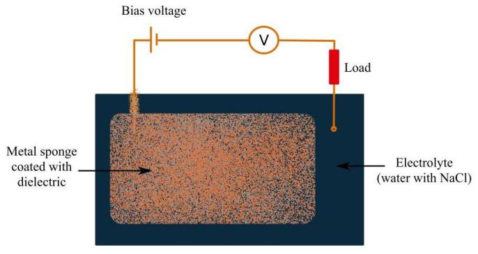
At first, all the metal electrode and electrolyte are on other sides of the dielectric coating (on the metal electrode sponge). This means the capacitance is high.

enter image description here

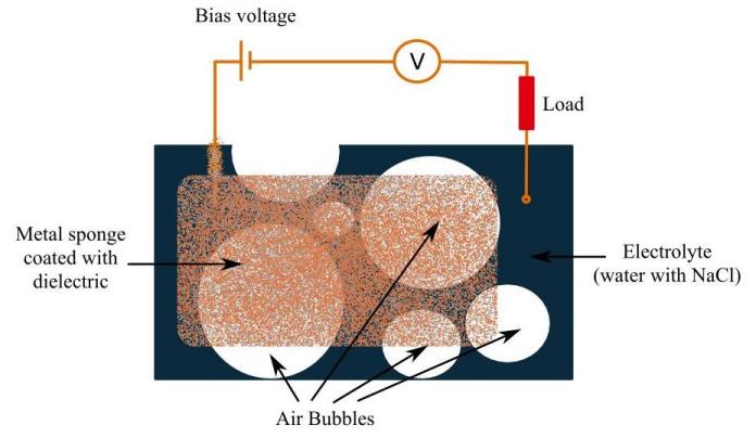
Then the air bubbles, which are non-conducting, displace the electrolyte and that causes the capacitance of the metal-dielectric-electrolyte interface to drop dramatically. Current will flow in the circuit.

EDIT 1: Given user @vir's comment about this being more about fluid dynamics than electronics, I want to clarify my diagram is NOT to scale! My question is about whether a huge surface area will improve the device as I expect it to, or will some other physical phenomenon come into play which will limit (or decrease) the expected power? The actual design could be adjusted if fluid dynamics predicts that bubbles cannot displace the electrolyte deep in the sponge.

enter image description here

I read this research paper and it uses bubbles to change the electrolyte and electrode interface, thus causing a change in capacitance as the bubble forms and exits the electrolyte.

For reference: https://www.nature.com/articles/srep16537

My question is why these guys didn't simply make a dielectric coated metal sponge submerged in electrolyte and create bubbles in that? Why use a "REWOD chip" that is only providing a planar interface for capacitance? I think the greater change in capacitance for each bubble, the greater the power will be. Shouldn't my design work better and if yes, then why did these guys go through the pain of making delicate chips with precision machines if they could simply sinter metal and coat it with some dielectric and submerge it into salt water?

I drew some diagrams here to demonstrate:

At first, all the metal electrode and electrolyte are on other sides of the dielectric coating (on the metal electrode sponge). This means the capacitance is high.

enter image description here

Then the air bubbles, which are non-conducting, displace the electrolyte and that causes the capacitance of the metal-dielectric-electrolyte interface to drop dramatically. Current will flow in the circuit.

enter image description here

I read this research paper and it uses bubbles to change the electrolyte and electrode interface, thus causing a change in capacitance as the bubble forms and exits the electrolyte.

For reference: https://www.nature.com/articles/srep16537

My question is why these guys didn't simply make a dielectric coated metal sponge submerged in electrolyte and create bubbles in that? Why use a "REWOD chip" that is only providing a planar interface for capacitance? I think the greater change in capacitance for each bubble, the greater the power will be. Shouldn't my design work better and if yes, then why did these guys go through the pain of making delicate chips with precision machines if they could simply sinter metal and coat it with some dielectric and submerge it into salt water?

I drew some diagrams here to demonstrate:

At first, all the metal electrode and electrolyte are on other sides of the dielectric coating (on the metal electrode sponge). This means the capacitance is high.

enter image description here

Then the air bubbles, which are non-conducting, displace the electrolyte and that causes the capacitance of the metal-dielectric-electrolyte interface to drop dramatically. Current will flow in the circuit.

EDIT 1: Given user @vir's comment about this being more about fluid dynamics than electronics, I want to clarify my diagram is NOT to scale! My question is about whether a huge surface area will improve the device as I expect it to, or will some other physical phenomenon come into play which will limit (or decrease) the expected power? The actual design could be adjusted if fluid dynamics predicts that bubbles cannot displace the electrolyte deep in the sponge.
enter image description here

Source Link
El Flea
  • 125
  • 5

Reverse electrowetting on dieletric using air bubble displacement for electricity generation

I read this research paper and it uses bubbles to change the electrolyte and electrode interface, thus causing a change in capacitance as the bubble forms and exits the electrolyte.

For reference: https://www.nature.com/articles/srep16537

My question is why these guys didn't simply make a dielectric coated metal sponge submerged in electrolyte and create bubbles in that? Why use a "REWOD chip" that is only providing a planar interface for capacitance? I think the greater change in capacitance for each bubble, the greater the power will be. Shouldn't my design work better and if yes, then why did these guys go through the pain of making delicate chips with precision machines if they could simply sinter metal and coat it with some dielectric and submerge it into salt water?

I drew some diagrams here to demonstrate:

At first, all the metal electrode and electrolyte are on other sides of the dielectric coating (on the metal electrode sponge). This means the capacitance is high.

enter image description here

Then the air bubbles, which are non-conducting, displace the electrolyte and that causes the capacitance of the metal-dielectric-electrolyte interface to drop dramatically. Current will flow in the circuit.

enter image description here