added 561 characters in body; edited title
Source Link
ocrdu
  • 9.3k
  • 23
  • 32
  • 42

I2C Level Shifter Isolationlevel shifter isolation

I am designing an FPGA-based SOM. There are I2C slave and master devices on the board. The I2C bus on the board includes an MCU that acts as a system manager and a bridge from UART to I2C, a PMIC device configured by I2C, a component containing an RTC and Temperaturetemperature sensor, the FPGA itself, the clock generator, and the output to the external environment from the mezzanine connector outside the board. 

The FPGA has a power-up sequence. FPGA IOs are not supposed to rise before the VCCIO voltage. So, so I have to go to isolation on the bus. For this reason, I decided to make a simple MOSFET-based level shifter so that it would take up little space and be cheap. 

I made a spiceSPICE simulation for a component containing two N-channel MOSFETs in a single package. The line was designed to meet the fast mode-mode I2C standard. Already the RTC/temperature sensor component and FPGA are using 1.8V,8 V; other devices are using 3.3V3 V.

In theory, I should be able to provide both isolation and level shifting. Because, because if 1.8V8 V VCCIO is not available, the MOSFETs will be cut off and there will be no leakage from the 3.3V3 V I2C line to the FPGA pin (a leak that may cause problems). 

However, in the simulation, I made with the SpiceSPICE model offered by the manufacturer of the MOSFET, while there is no problem during normal operation when VCCIO is removed and there is no switching on the 3.3V3 V side, 3.1 odd volts-odd V leakage appears on the FPGA side. Additionally, if there is switching on the 3.3V3 V side when there is no VCCIO, I still read 1.8V8 V on the FPGA side.

What exactly do you think is the reason for this? Am I missing something? What are your possible solution suggestions?

Note: All parasitics on the bus were made taking into account the FPGA's IBIS model, component datasheets, and possible path widths and lengths in the PCB stack.

Normal operation is the same for SCL and SDA: Normal operation is the same for SCL and SDA.Normal operation is the same for SCL and SDA
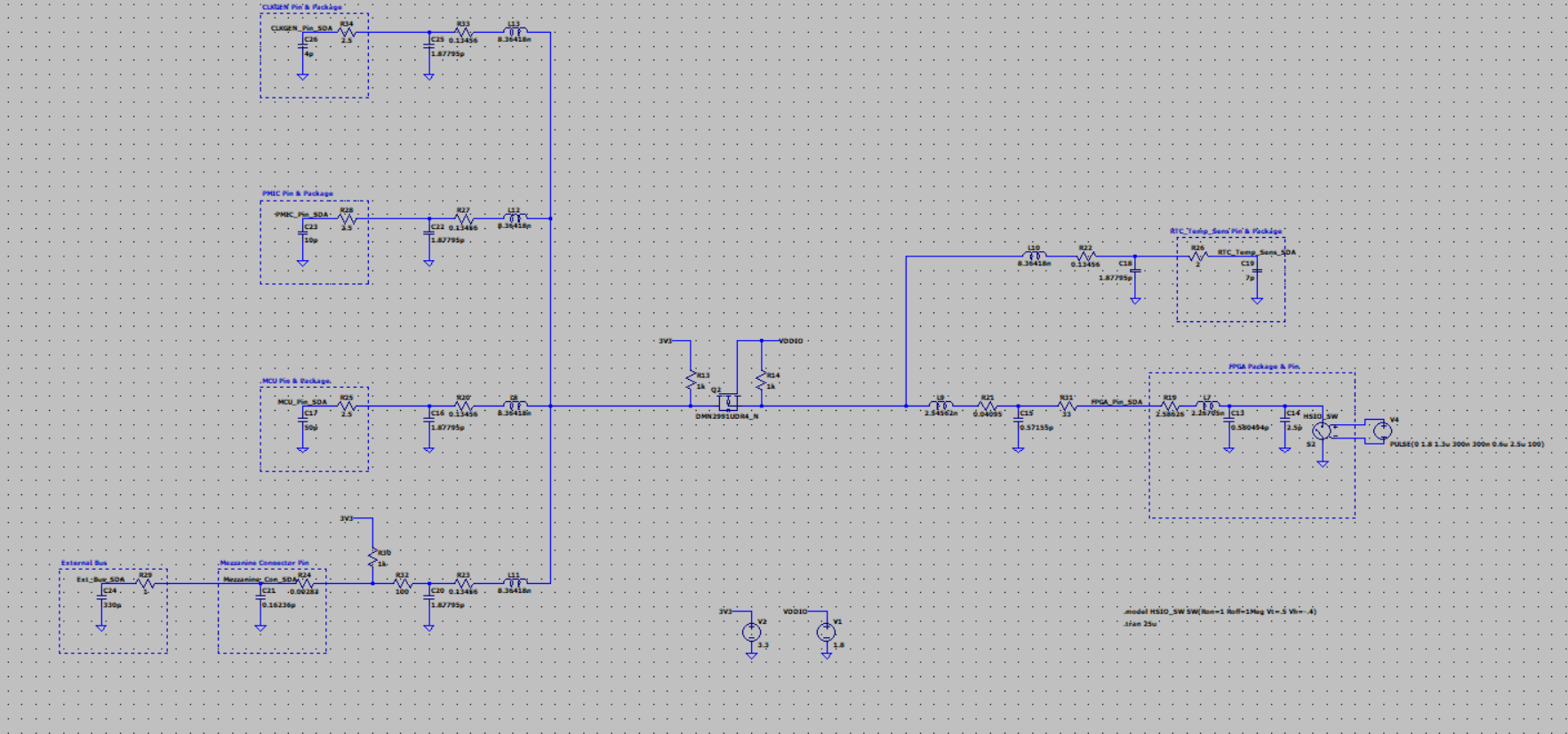
Normal operation, VCCIO side waveform: Normal operation, VCCIO side waveform

Normal operation, 3.3 V side waveform: Normal operation, 3.3V side waveformNormal operation, 3.3 V side waveform

With no VCCIO (floating) and no switching: With no VCCIO (floating) and no switching

VCCIO side waveform with no VCCIO (floating) and no switching (3.3 V side already showing flat 3.3 V): VCCIO side waveform with no VCCIO (floating) and no switching (3.3V side already showing flat 3.3V)VCCIO side waveform with no VCCIO (floating) and no switching (3.3 V side already showing flat 3.3 V)

Transistor drain current waveform with no VCCIO (floating) and no switching on the 3.3 V side: Transistor drain current waveform with no VCCIO (floating) and no switching on the 3.3V sideTransistor drain current waveform with no VCCIO (floating) and no switching on the 3.3 V side

When there is no VCCIO (floating) and there is switching on the 3.3 V side: When there is no VCCIO (floating) and there is switching on the 3.3V sideWhen there is no VCCIO (floating) and there is switching on the 3.3 V side

VCCIO side waveform with no VCCIO (floating) and 3.3 V side switching (3.3 V side same as normal operation): VCCIO side waveform with no VCCIO (floating) and 3.3V side switching (3.3V side same as normal operation)VCCIO side waveform with no VCCIO (floating) and 3.3 V side switching (3.3 V side same as normal operation)

I2C Level Shifter Isolation

I am designing an FPGA-based SOM. There are I2C slave and master devices on the board. The I2C bus on the board includes an MCU that acts as a system manager and a bridge from UART to I2C, a PMIC device configured by I2C, a component containing RTC and Temperature sensor, the FPGA itself, the clock generator and the output to the external environment from the mezzanine connector outside the board. The FPGA has a power-up sequence. FPGA IOs are not supposed to rise before the VCCIO voltage. So I have to go to isolation on the bus. For this reason, I decided to make a simple MOSFET-based level shifter so that it would take up little space and be cheap. I made a spice simulation for a component containing two N-channel MOSFETs in a single package. The line was designed to meet the fast mode I2C standard. Already the RTC/temperature sensor component and FPGA are using 1.8V, other devices are using 3.3V.

In theory, I should be able to provide both isolation and level shifting. Because if 1.8V VCCIO is not available, the MOSFETs will be cut off and there will be no leakage from the 3.3V I2C line to the FPGA pin (a leak that may cause problems). However, in the simulation, I made with the Spice model offered by the manufacturer of the MOSFET, while there is no problem during normal operation when VCCIO is removed and there is no switching on the 3.3V side, 3.1 odd volts leakage appears on the FPGA side. Additionally, if there is switching on the 3.3V side when there is no VCCIO, I still read 1.8V on the FPGA side.

What exactly do you think is the reason for this? Am I missing something? What are your possible solution suggestions?

Note: All parasitics on the bus were made taking into account the FPGA's IBIS model, component datasheets, and possible path widths and lengths in the PCB stack.

Normal operation is the same for SCL and SDA.

Normal operation, VCCIO side waveform

Normal operation, 3.3V side waveform

With no VCCIO (floating) and no switching

VCCIO side waveform with no VCCIO (floating) and no switching (3.3V side already showing flat 3.3V)

Transistor drain current waveform with no VCCIO (floating) and no switching on the 3.3V side

When there is no VCCIO (floating) and there is switching on the 3.3V side

VCCIO side waveform with no VCCIO (floating) and 3.3V side switching (3.3V side same as normal operation)

I2C level shifter isolation

I am designing an FPGA-based SOM. There are I2C slave and master devices on the board. The I2C bus on the board includes an MCU that acts as a system manager and a bridge from UART to I2C, a PMIC device configured by I2C, a component containing an RTC and temperature sensor, the FPGA itself, the clock generator, and the output to the external environment from the mezzanine connector outside the board. 

The FPGA has a power-up sequence. FPGA IOs are not supposed to rise before the VCCIO voltage, so I have to go to isolation on the bus. For this reason, I decided to make a simple MOSFET-based level shifter so that it would take up little space and be cheap. 

I made a SPICE simulation for a component containing two N-channel MOSFETs in a single package. The line was designed to meet the fast-mode I2C standard. Already the RTC/temperature sensor component and FPGA are using 1.8 V; other devices are using 3.3 V.

In theory, I should be able to provide both isolation and level shifting, because if 1.8 V VCCIO is not available, the MOSFETs will be cut off and there will be no leakage from the 3.3 V I2C line to the FPGA pin (a leak that may cause problems). 

However, in the simulation I made with the SPICE model offered by the manufacturer of the MOSFET, while there is no problem during normal operation when VCCIO is removed and there is no switching on the 3.3 V side, 3.1-odd V leakage appears on the FPGA side. Additionally, if there is switching on the 3.3 V side when there is no VCCIO, I still read 1.8 V on the FPGA side.

What exactly do you think is the reason for this? Am I missing something? What are your possible solution suggestions?

Note: All parasitics on the bus were made taking into account the FPGA's IBIS model, component datasheets, and possible path widths and lengths in the PCB stack.

Normal operation is the same for SCL and SDA: Normal operation is the same for SCL and SDA

Normal operation, VCCIO side waveform: Normal operation, VCCIO side waveform

Normal operation, 3.3 V side waveform: Normal operation, 3.3 V side waveform

With no VCCIO (floating) and no switching: With no VCCIO (floating) and no switching
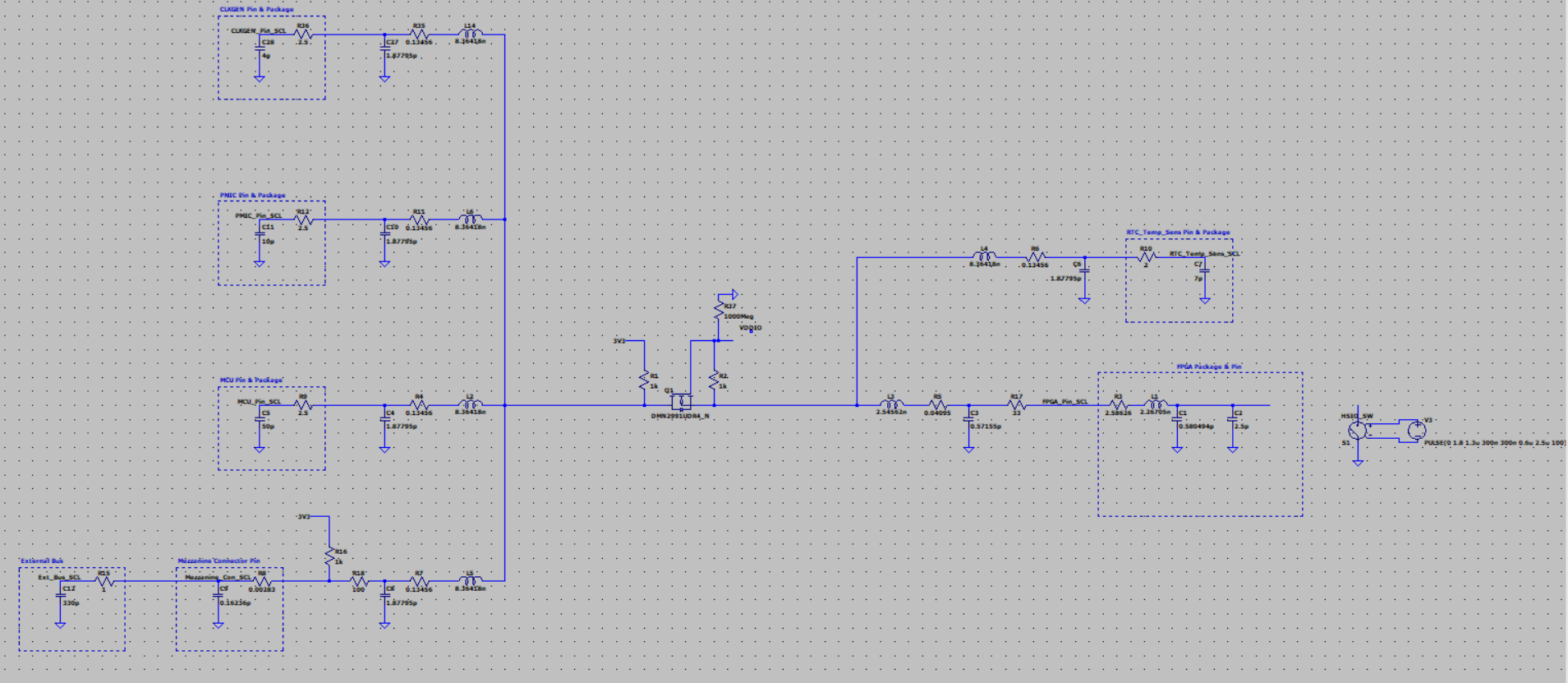
VCCIO side waveform with no VCCIO (floating) and no switching (3.3 V side already showing flat 3.3 V): VCCIO side waveform with no VCCIO (floating) and no switching (3.3 V side already showing flat 3.3 V)

Transistor drain current waveform with no VCCIO (floating) and no switching on the 3.3 V side: Transistor drain current waveform with no VCCIO (floating) and no switching on the 3.3 V side

When there is no VCCIO (floating) and there is switching on the 3.3 V side: When there is no VCCIO (floating) and there is switching on the 3.3 V side
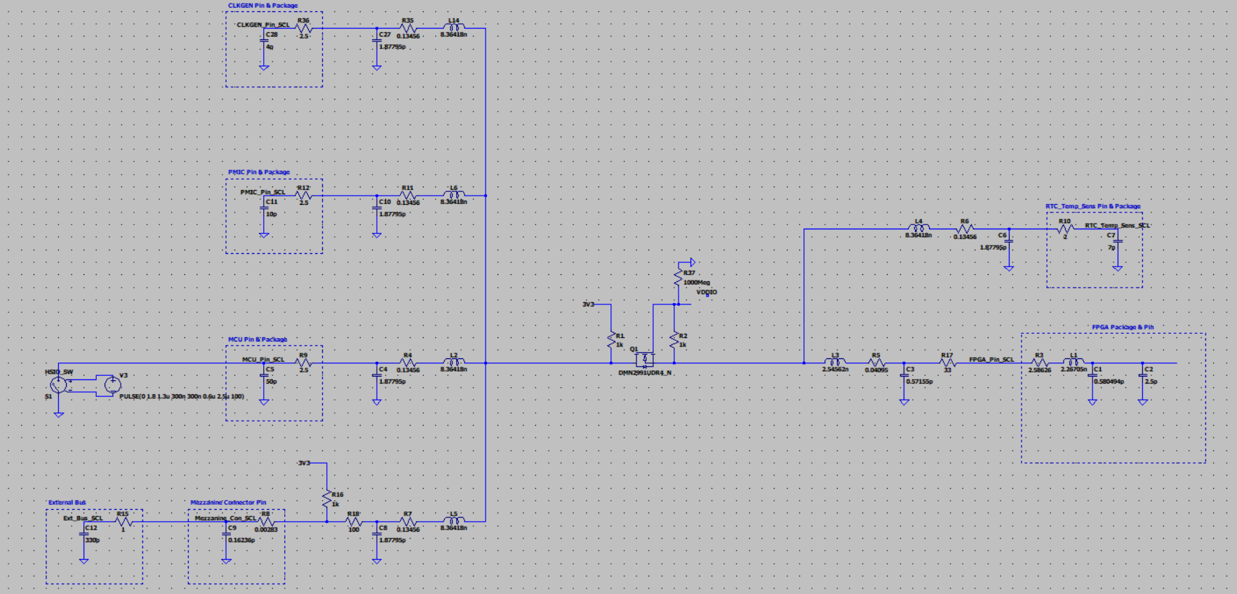
VCCIO side waveform with no VCCIO (floating) and 3.3 V side switching (3.3 V side same as normal operation): VCCIO side waveform with no VCCIO (floating) and 3.3 V side switching (3.3 V side same as normal operation)

added 4 characters in body
Source Link

I am designing an FPGA-based SOM. There are I2C slave and master devices on the board. The I2C bus on the board includes an MCU that acts as a system manager and a bridge from UART to I2C, a PMIC device configured by I2C, a component containing RTC and Temperature sensor, the FPGA itself, the clock generator and the output to the external environment from the mezzanine connector outside the board. The FPGA has a power-up sequence. FPGA IOs are not supposed to rise before the VCCIO voltage. So I have to go to isolation on the bus. For this reason, I decided to make a simple MOSFET-based level shifter so that it would take up little space and be cheap. I made a spice simulation for a component containing two N-channel MOSFETs in a single package. The line was designed to meet the fast mode I2C standard. Already the RTC/temperature sensor component and FPGA are using 1.8V, other devices are using 3.3V.

In theory, I should be able to provide both isolation and level shifting. Because if 1.8V VCCIO is not available, the MOSFETs will be cut off and there will be no leakage from the 3.3V I2C line to the FPGA pin (a leak that may cause problems). However, in the simulation, I made with the Spice model offered by the manufacturer of the MOSFET, while there is no problem during normal operation when VCCIO is removed and there is no switching on the 3.3V side, 3.1 odd volts leakage appears on the FPGA side. Additionally, if there is switching on the 3.3V side when there is no VCCIO, I still read 1.8V on the FPGA side.

What exactly do you think is the reason for this? Am I missing something? What are your possible solution suggestions?

Note: All parasitics on the bus were made taking into account the FPGA's IBIS model, component datasheets, and possible path widths and lengths in the PCB stack. 

Normal operation is the same for SCL and SDA.

Normal operation, VCCIO side waveform

Normal operation, 3.3V side waveform

With no VCCIO (floating) and no switching

VCCIO side waveform with no VCCIO (floating) and no switching (3.3V side already showing flat 3.3V)

Transistor drain current waveform with no VCCIO (floating) and no switching on the 3.3V side

When there is no VCCIO (floating) and there is switching on the 3.3V side

VCCIO side waveform with no VCCIO (floating) and 3.3V side switching (3.3V side same as normal operation)

I am designing an FPGA-based SOM. There are I2C slave and master devices on the board. The I2C bus on the board includes an MCU that acts as a system manager and a bridge from UART to I2C, a PMIC device configured by I2C, a component containing RTC and Temperature sensor, the FPGA itself, the clock generator and the output to the external environment from the mezzanine connector outside the board. The FPGA has a power-up sequence. FPGA IOs are not supposed to rise before the VCCIO voltage. So I have to go to isolation on the bus. For this reason, I decided to make a simple MOSFET-based level shifter so that it would take up little space and be cheap. I made a spice simulation for a component containing two N-channel MOSFETs in a single package. The line was designed to meet the fast mode I2C standard. Already the RTC/temperature sensor component and FPGA are using 1.8V, other devices are using 3.3V.

In theory, I should be able to provide both isolation and level shifting. Because if 1.8V VCCIO is not available, the MOSFETs will be cut off and there will be no leakage from the 3.3V I2C line to the FPGA pin (a leak that may cause problems). However, in the simulation, I made with the Spice model offered by the manufacturer of the MOSFET, while there is no problem during normal operation when VCCIO is removed and there is no switching on the 3.3V side, 3.1 odd volts leakage appears on the FPGA side. Additionally, if there is switching on the 3.3V side when there is no VCCIO, I still read 1.8V on the FPGA side.

What exactly do you think is the reason for this? Am I missing something? What are your possible solution suggestions?

Note: All parasitics on the bus were made taking into account the FPGA's IBIS model, component datasheets, and possible path widths and lengths in the PCB stack.Normal operation is the same for SCL and SDA.

Normal operation, VCCIO side waveform

Normal operation, 3.3V side waveform

With no VCCIO (floating) and no switching

VCCIO side waveform with no VCCIO (floating) and no switching (3.3V side already showing flat 3.3V)

Transistor drain current waveform with no VCCIO (floating) and no switching on the 3.3V side

When there is no VCCIO (floating) and there is switching on the 3.3V side

VCCIO side waveform with no VCCIO (floating) and 3.3V side switching (3.3V side same as normal operation)

I am designing an FPGA-based SOM. There are I2C slave and master devices on the board. The I2C bus on the board includes an MCU that acts as a system manager and a bridge from UART to I2C, a PMIC device configured by I2C, a component containing RTC and Temperature sensor, the FPGA itself, the clock generator and the output to the external environment from the mezzanine connector outside the board. The FPGA has a power-up sequence. FPGA IOs are not supposed to rise before the VCCIO voltage. So I have to go to isolation on the bus. For this reason, I decided to make a simple MOSFET-based level shifter so that it would take up little space and be cheap. I made a spice simulation for a component containing two N-channel MOSFETs in a single package. The line was designed to meet the fast mode I2C standard. Already the RTC/temperature sensor component and FPGA are using 1.8V, other devices are using 3.3V.

In theory, I should be able to provide both isolation and level shifting. Because if 1.8V VCCIO is not available, the MOSFETs will be cut off and there will be no leakage from the 3.3V I2C line to the FPGA pin (a leak that may cause problems). However, in the simulation, I made with the Spice model offered by the manufacturer of the MOSFET, while there is no problem during normal operation when VCCIO is removed and there is no switching on the 3.3V side, 3.1 odd volts leakage appears on the FPGA side. Additionally, if there is switching on the 3.3V side when there is no VCCIO, I still read 1.8V on the FPGA side.

What exactly do you think is the reason for this? Am I missing something? What are your possible solution suggestions?

Note: All parasitics on the bus were made taking into account the FPGA's IBIS model, component datasheets, and possible path widths and lengths in the PCB stack. 

Normal operation is the same for SCL and SDA.

Normal operation, VCCIO side waveform

Normal operation, 3.3V side waveform

With no VCCIO (floating) and no switching

VCCIO side waveform with no VCCIO (floating) and no switching (3.3V side already showing flat 3.3V)

Transistor drain current waveform with no VCCIO (floating) and no switching on the 3.3V side

When there is no VCCIO (floating) and there is switching on the 3.3V side

VCCIO side waveform with no VCCIO (floating) and 3.3V side switching (3.3V side same as normal operation)

Source Link

I2C Level Shifter Isolation

I am designing an FPGA-based SOM. There are I2C slave and master devices on the board. The I2C bus on the board includes an MCU that acts as a system manager and a bridge from UART to I2C, a PMIC device configured by I2C, a component containing RTC and Temperature sensor, the FPGA itself, the clock generator and the output to the external environment from the mezzanine connector outside the board. The FPGA has a power-up sequence. FPGA IOs are not supposed to rise before the VCCIO voltage. So I have to go to isolation on the bus. For this reason, I decided to make a simple MOSFET-based level shifter so that it would take up little space and be cheap. I made a spice simulation for a component containing two N-channel MOSFETs in a single package. The line was designed to meet the fast mode I2C standard. Already the RTC/temperature sensor component and FPGA are using 1.8V, other devices are using 3.3V.

In theory, I should be able to provide both isolation and level shifting. Because if 1.8V VCCIO is not available, the MOSFETs will be cut off and there will be no leakage from the 3.3V I2C line to the FPGA pin (a leak that may cause problems). However, in the simulation, I made with the Spice model offered by the manufacturer of the MOSFET, while there is no problem during normal operation when VCCIO is removed and there is no switching on the 3.3V side, 3.1 odd volts leakage appears on the FPGA side. Additionally, if there is switching on the 3.3V side when there is no VCCIO, I still read 1.8V on the FPGA side.

What exactly do you think is the reason for this? Am I missing something? What are your possible solution suggestions?

Note: All parasitics on the bus were made taking into account the FPGA's IBIS model, component datasheets, and possible path widths and lengths in the PCB stack.Normal operation is the same for SCL and SDA.

Normal operation, VCCIO side waveform

Normal operation, 3.3V side waveform

With no VCCIO (floating) and no switching

VCCIO side waveform with no VCCIO (floating) and no switching (3.3V side already showing flat 3.3V)

Transistor drain current waveform with no VCCIO (floating) and no switching on the 3.3V side

When there is no VCCIO (floating) and there is switching on the 3.3V side

VCCIO side waveform with no VCCIO (floating) and 3.3V side switching (3.3V side same as normal operation)