added 5 characters in body
Source Link

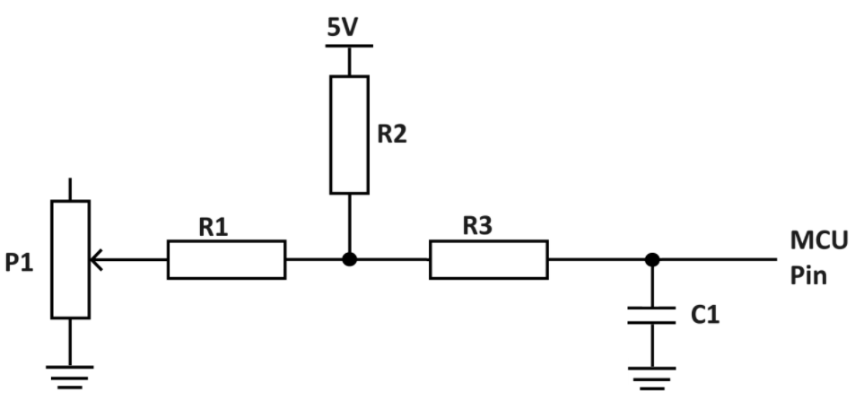
I am having a bit of a hard time understanding the voltage read in the voltage divider that is being an input for an ADC to an NXP microcontroller, S32K118. Below is the schematic of the circuit.

circuit schematicschematic of the circuit

Where P1 and R1 represent an analogic temperature sensor, just for hardware debugging purposes.

The designed and the real values of each component are represented in the table below:

Component Design Real
P1 10k Ohms 9.4k Ohms
R1 4.7k Ohms 4.4k Ohms
R2 15k Ohms 13.4k Ohms
R3 22k Ohms 21.9k Ohms
C1 100n F 100n F

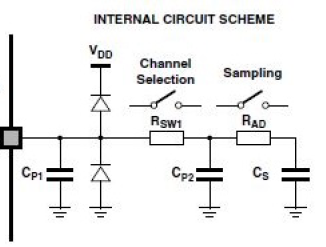
According to the MCU (S32Kxx) datasheet, the ADC input impedance equivalency diagram is shown below:

ADC input impedance equivalency

As the signal from the sensor is updated at a very slow rate, I consider the signal being DC, therefore no current flows into the ADC pin and the voltage at the node (R1,R2 & R3) is the same as in the node (R3 & C1).

Then, calculating the voltage divider in both cases, which resistance of the potentiometer was changed from the minimum to the maximum, using the real values, I got the following values:

$$ Vout = \frac{(P1 + R1)}{(P1 + R1) + R2}{Vin} $$

V_{in} = 5V

Vout_{min} = 1.23V

Vout_{max} = 2.45V

However, the values that I am reading with the multimeter are:

Vout_{min} = 0.22V

Vout_{max} = 0.65V

That makes no sense, I have checked all the tracks and components, and they are in order.

Am I missing some point that is leading to misunderstanding something?

I am having a bit of a hard time understanding the voltage read in the voltage divider that is being an input for an ADC to an NXP microcontroller, S32K118. Below is the schematic of the circuit.

circuit schematic

Where P1 and R1 represent an analogic temperature sensor, just for hardware debugging purposes.

The designed and the real values of each component are represented in the table below:

Component Design Real
P1 10k Ohms 9.4k Ohms
R1 4.7k Ohms 4.4k Ohms
R2 15k Ohms 13.4k Ohms
R3 22k Ohms 21.9k Ohms
C1 100n F 100n F

According to the MCU (S32Kxx) datasheet, the ADC input impedance equivalency diagram is shown below:

ADC input impedance equivalency

As the signal from the sensor is updated at a very slow rate, I consider the signal being DC, therefore no current flows into the ADC pin and the voltage at the node (R1,R2 & R3) is the same as in the node (R3 & C1).

Then, calculating the voltage divider in both cases, which resistance of the potentiometer was changed from the minimum to the maximum, using the real values, I got the following values:

$$ Vout = \frac{(P1 + R1)}{(P1 + R1) + R2}{Vin} $$

V_{in} = 5V

Vout_{min} = 1.23V

Vout_{max} = 2.45V

However, the values that I am reading with the multimeter are:

Vout_{min} = 0.22V

Vout_{max} = 0.65V

That makes no sense, I have checked all the tracks and components, and they are in order.

Am I missing some point that is leading to misunderstanding something?
I am having a bit of a hard time understanding the voltage read in the voltage divider that is being an input for an ADC to an NXP microcontroller, S32K118. Below is the schematic of the circuit.

schematic of the circuit

Where P1 and R1 represent an analogic temperature sensor, just for hardware debugging purposes.

The designed and the real values of each component are represented in the table below:

Component Design Real
P1 10k Ohms 9.4k Ohms
R1 4.7k Ohms 4.4k Ohms
R2 15k Ohms 13.4k Ohms
R3 22k Ohms 21.9k Ohms
C1 100n F 100n F

According to the MCU (S32Kxx) datasheet, the ADC input impedance equivalency diagram is shown below:

ADC input impedance equivalency

As the signal from the sensor is updated at a very slow rate, I consider the signal being DC, therefore no current flows into the ADC pin and the voltage at the node (R1,R2 & R3) is the same as in the node (R3 & C1).

Then, calculating the voltage divider in both cases, which resistance of the potentiometer was changed from the minimum to the maximum, using the real values, I got the following values:

$$ Vout = \frac{(P1 + R1)}{(P1 + R1) + R2}{Vin} $$

V_{in} = 5V

Vout_{min} = 1.23V

Vout_{max} = 2.45V

However, the values that I am reading with the multimeter are:

Vout_{min} = 0.22V

Vout_{max} = 0.65V

That makes no sense, I have checked all the tracks and components, and they are in order.

Am I missing some point that is leading to misunderstanding something?
edited tags
Link
added Vin value
Source Link

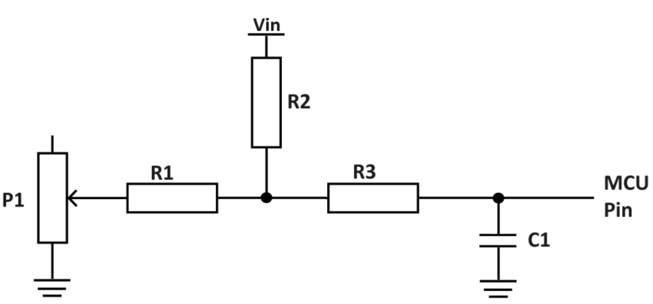
I am having a bit of a hard time understanding the voltage read in the voltage divider that is being an input for an ADC to an NXP microcontroller, S32K118. Below is the schematic of the circuit.

circuit schematic

Where P1 and R1 represent an analogic temperature sensor, just for hardware debugging purposes.

The designed and the real values of each component are represented in the table below: | Component| Design | Real | | :----: |:------: | :-----: | | P1 | 10k Ohms| 9.4k Ohms| | R1 | 4.7k Ohms| 4.4k Ohms| | R2 | 15k Ohms| 13.4k Ohms| | R3 | 22k Ohms| 21.9k Ohms| | C1 | 100n F | 100n F |

ComponentDesignReal
P110k Ohms9.4k Ohms
R14.7k Ohms4.4k Ohms
R215k Ohms13.4k Ohms
R322k Ohms21.9k Ohms
C1100n F100n F

According to the MCU (S32Kxx) datasheet, the ADC input impedance equivalency diagram is shown below:

ADC input impedance equivalency

As the signal from the sensor is updated at a very slow rate, I consider the signal being DC, therefore no current flows into the ADC pin and the voltage at the node (R1,R2 & R3) is the same as in the node (R3 & C1).

Then, calculating the voltage divider in both cases, which resistance of the potentiometer was changed from the minimum to the maximum, using the real values, I got the following values:

$$ Vout = \frac{(P1 + R1)}{(P1 + R1) + R2}{Vin} $$

V_{in} = 5V

Vout_{min} = 1.23V

Vout_{max} = 2.45V

However, the values that I am reading with the multimeter are:

Vout_{min} = 0.22V

Vout_{max} = 0.65V

That makes no sense, I have checked all the tracks and components, and they are in order.

Am I missing some point that is leading to misunderstanding something?
I am having a bit of a hard time understanding the voltage read in the voltage divider that is being an input for an ADC to an NXP microcontroller, S32K118. Below is the schematic of the circuit.

circuit schematic

Where P1 and R1 represent an analogic temperature sensor, just for hardware debugging purposes.

The designed and the real values of each component are represented in the table below: | Component| Design | Real | | :----: |:------: | :-----: | | P1 | 10k Ohms| 9.4k Ohms| | R1 | 4.7k Ohms| 4.4k Ohms| | R2 | 15k Ohms| 13.4k Ohms| | R3 | 22k Ohms| 21.9k Ohms| | C1 | 100n F | 100n F |

According to the MCU (S32Kxx) datasheet, the ADC input impedance equivalency diagram is shown below:

ADC input impedance equivalency

As the signal from the sensor is updated at a very slow rate, I consider the signal being DC, therefore no current flows into the ADC pin and the voltage at the node (R1,R2 & R3) is the same as in the node (R3 & C1).

Then, calculating the voltage divider in both cases, which resistance of the potentiometer was changed from the minimum to the maximum, using the real values, I got the following values:

$$ Vout = \frac{(P1 + R1)}{(P1 + R1) + R2}{Vin} $$

Vout_{min} = 1.23V

Vout_{max} = 2.45V

However, the values that I am reading with the multimeter are:

Vout_{min} = 0.22V

Vout_{max} = 0.65V

That makes no sense, I have checked all the tracks and components, and they are in order.

Am I missing some point that is leading to misunderstanding something?

I am having a bit of a hard time understanding the voltage read in the voltage divider that is being an input for an ADC to an NXP microcontroller, S32K118. Below is the schematic of the circuit.

circuit schematic

Where P1 and R1 represent an analogic temperature sensor, just for hardware debugging purposes.

The designed and the real values of each component are represented in the table below:

ComponentDesignReal
P110k Ohms9.4k Ohms
R14.7k Ohms4.4k Ohms
R215k Ohms13.4k Ohms
R322k Ohms21.9k Ohms
C1100n F100n F

According to the MCU (S32Kxx) datasheet, the ADC input impedance equivalency diagram is shown below:

ADC input impedance equivalency

As the signal from the sensor is updated at a very slow rate, I consider the signal being DC, therefore no current flows into the ADC pin and the voltage at the node (R1,R2 & R3) is the same as in the node (R3 & C1).

Then, calculating the voltage divider in both cases, which resistance of the potentiometer was changed from the minimum to the maximum, using the real values, I got the following values:

$$ Vout = \frac{(P1 + R1)}{(P1 + R1) + R2}{Vin} $$

V_{in} = 5V

Vout_{min} = 1.23V

Vout_{max} = 2.45V

However, the values that I am reading with the multimeter are:

Vout_{min} = 0.22V

Vout_{max} = 0.65V

That makes no sense, I have checked all the tracks and components, and they are in order.

Am I missing some point that is leading to misunderstanding something?

Source Link
Loading