Conceptually Simple Current Source
When considering a circuit that creates a current source from a low impedance voltage source, perhaps the easiest to conceive is this:

simulate this circuit – Schematic created using CircuitLab
The current regulation of this circuit, with respect to changes in the load, is:
$$\%\,I_\text{LOAD} = \left[\frac{-1}{1+\frac{R_\text{DROP}}{R_\text{LOAD}}}\right]\cdot \%\,R_\text{LOAD}$$
In short, the larger \$R_\text{DROP}\$ is the better. But this means that \$V_\text{SRC}\$ needs to be larger. So, a nearly ideal current source can be fabricated from a very, very high voltage source and a corresponding very, very large voltage-dropping resistor.
For example, suppose \$R_\text{LOAD}=100\:\Omega\$ and you want a constant current of \$I_\text{LOAD}=100\:\text{mA}\$. You could use \$V_\text{SRC}=100\:\text{V}\$ and \$R_\text{DROP}=\frac{V_\text{SRC}-R_\text{LOAD}\cdot I_\text{LOAD}}{I_\text{LOAD}}=990\:\Omega\$. This would provide regulation equivalent to about \$\%\,I_\text{LOAD} = 0.092\cdot \%\,R_\text{LOAD}\$. A 10% increase in \$R_\text{LOAD}\$ would exhibit only a -0.9% variation in \$I_\text{LOAD}\$, or a change of about \$-900\:\mu\text{A}\$ to \$I_\text{LOAD}\approx 99.1\:\text{mA}\$. The price is that you need a higher voltage supply (which is more complex) and have to waste an additional \$9.9\:\text{W}\$ in the dropping resistor to deliver a constant current into a roughly \$1\:\text{W}\$ load.
That may be good enough. Who can say? But it's simple to conceive. And it is very easy to see how to improve the current regulation with respect to load changes. Just use a still higher voltage for your power supply and a larger valued dropping resistor to go along with it and waste still more power (and add complexity and safety issues.)
This method is very commonly used when the load is an LED. In part, this is because the LED is a non-linear device and in part this is also because the regulation needs for LEDs are often fairly loose, so a lower voltage works well enough for the purposes. But it's also a pretty bad choice in other cases.
Your Circuits
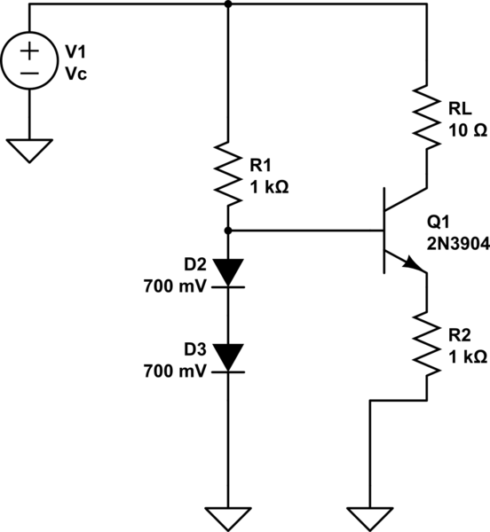
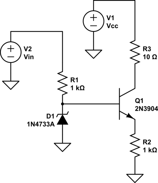
Below left is one, below right is another, and I've added the middle one to act as a transition schematic between the two (mostly because it's commonly found in practice):

simulate this circuit
I won't spend a lot of time on them. Just a few points.
The schematic on the left has an advantage of a wider compliance voltage range for the load, because two diode drops aren't a lot of overhead -- leaving more of the available supply voltage for the load. But diodes vary a fair amount, one to another, and their voltage drop is highly affected by ambient temperature and, to a degree, by the current in them as well. Variations in the load lead to variations in the base current of the BJT and impact to a small degree the current in the diodes, as well. Those load variations, as well as temperature, also affect the BJT's base-emitter voltage and that also impacts the load current.
The middle schematic is used because it doesn't require two voltage supplies. That's an advantage. But it also has the disadvantage that the current in the zener can vary widely and this does impact its voltage and therefore the load current.
The right hand schematic isn't found as often because of the dual-supply requirement. (This is the one you call your own invention.) But it does permit setting the zener current independently from the compliance voltage source used for the load. Still, the requirement for an extra voltage source is an annoyance.
While I've kept your idea as you wrote it, most of us would probably gravitate away from requiring a separate voltage supply and would, instead, more likely move towards replacing your zener's resistor with a constant current source tied to the original voltage rail. It achieves the goal without needing a new voltage rail. (Less parts, smaller, and probably lower power, as well.)
The disadvantage of both middle and right schematics, vs the left schematic, is the loss of voltage headroom. So there's a price to pay.
And all of them suffer from temperature variations, to some degree from part variations, and from the Early Effect in the BJT.
Two Additions to Consider
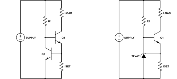
Here are two improvements:

simulate this circuit
The left side replaces your diodes or zener with an active BJT that measures the current in \$R_\text{ISET}\$ and makes adjustments to the base voltage of \$Q_1\$. This is much better because it also takes into account \$Q_1\$'s Early Effect by measuring it, too, and correcting for it. So this is a big improvement in that sense. However, it remains sensitive to \$Q_2\$'s temperature and part variations. It also is sensitive to the supply voltage because that can greatly increase the current in \$R_1\$ and thereby require higher collector currents in \$Q_2\$ which affects the base-emitter voltage and thereby also the collector current of \$Q_1\$. So it will still respond somewhat to wide swings in the supply voltage, causing load current variation with supply voltage. It's just a bit better on a few scores. And it can be better designed/managed, if you put some work into it.
It would be possible to consider replacing \$R_1\$ with an active current source -- just as I suggested one could also do with the earlier "middle" schematic and that would improve it's behavior with changes in the supply voltage. But it comes at the cost of added voltage overhead and more parts. So, like everything, there are trade-offs to consider.
Just a last note on the left side schematic. Although it does respond a lot to temperature variations in \$Q_2\$, it is relatively immune to temperature variations in \$Q_1\$. Since most of the power dissipation is in \$Q_1\$, which heats it up, and since it is possible (usually) to keep \$Q_2\$ at some distance from it, this helps limit the temperature response of the circuit to ambient changes and not to ambient changes plus thermal changes due to load or power supply variations. If one arranged for \$Q_1\$ to be thermally stable somehow, it would be pretty decent. Unfortunately, that would likely make the circuit unaffordably complex for the benefit.
The right side schematic is about as close to perfect as you are likely to find. The TLV431 device has a lot of internal parts and some very crafted design work so that it is relatively stable over a very very wide range of ambient temperatures. It just works. Period. It also works well over almost three magnitudes of operating current, so you can pretty much just use \$R_1\$ without worrying about replacing it with a current source, too. This makes this right side schematic almost like gold. It corrects for the Early Effect in \$Q_1\$, too, as well as temperature effects on \$Q_1\$, too.
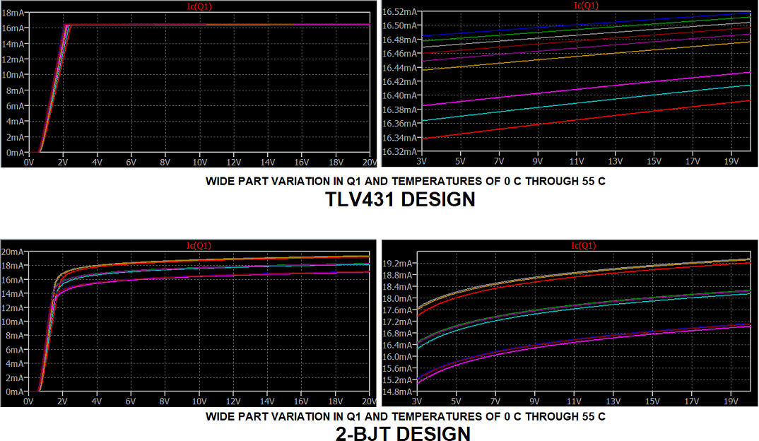
Here's a Spice run. I didn't vary the load, but I varied the operating temperature from \$0^\circ\text{C}\$ to \$55^\circ\text{C}\$ and varied \$Q_1\$ over quite a range of possible behaviors. The left side of the display below includes the entire supply voltage range from \$0\:\text{V}\$ to \$20\:\text{V}\$, while the right side shows the supply voltage range from \$3\:\text{V}\$ to \$20\:\text{V}\$ in order to zoom up on the variations better. Both the TLV431 and 2-BJT designs were set for about \$16\:\text{mA}\$, which I just picked out of the air for these purposes.
I think you can see the difference that a TLV431 makes.

Summary
Sensitivity equations are also very, very useful in helping to both quantitatively estimate how a variation of an input parameter impacts a design goal's output parameter. The process allows you to first find out which is of more concern and then also if that concern is sufficient to warrant more design effort. Or, alternately, to realize that that the design goals have been met and the design can be considered complete.
Another approach used by many is to just perform lots of Spice runs (or use lots of Excel runs) to achieve similar results.
Note: Pete W mentioned in a comment below that the LM4041 is a high-side device similar to the TLV431 device. I hadn't known about it and now I'm glad to hear of it. So I'm making a note about it within the answer to capture the option. Sometimes, you want a controllable high-side source rather than a sink, depending on load requirements. So that's a nice catch from Pete W. Thanks!
