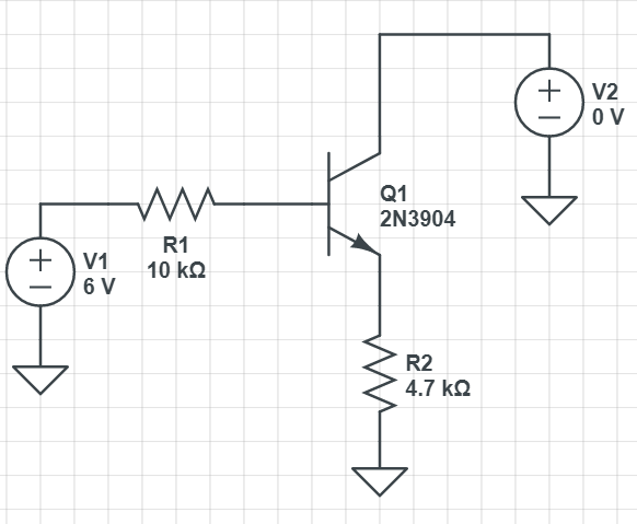
I try one example, say V2 = 0V. I thought there is a current goes from V1 to R1 to base to emitter to R2 to ground. But when I use simulation, I find that there is no current goes through R2, there is a current goes from R1 to base to collector to V2 to ground.
It's a NPN transistor, so both the base-emitter junction and the base-collector junction are a PN junction. So, under the right conditions, current can flow from base to collector as you've seen.
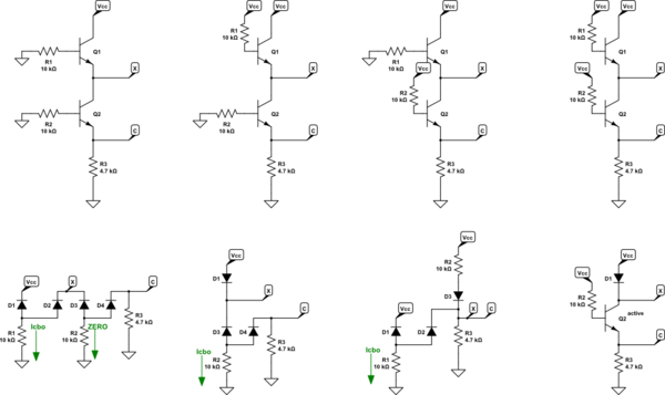
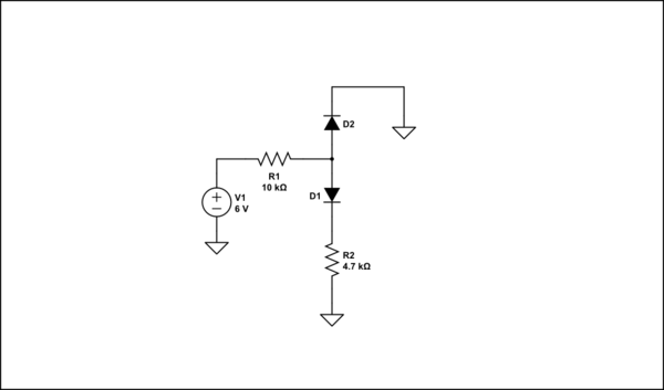
Below is a simplified version of your schematic to better illustrate why. The 2 PN junctions are replaced with diodes and the 0V V2 with ground. (because a 0V DC supply is equivalent to ground).

simulate this circuit – Schematic created using CircuitLab
Current can flow trough D2 straight to ground. The voltage at the anode will be about 0.6V above ground (D2's forward voltage). Any current flowing trough D1 and R2 causes a voltage drop in R2, which lifts D1's cathode voltage. Since it's anode is clamped at 0.6V by D2 there's not enough forward voltage to keep D1 conducting. Thus the bulk of the current will flow trough D2.
Note that this is a special situation, caused by the resistance in series with the emitter and forcing the collector voltage low enough, not something you'll see in actual circuits.
EDIT:
As you explain, I understood when V2 = 0. But how about V2 = 0.1V ; 0.2V ; 0.3V ; 0.4V...?
It's just as simple for other V2 voltages. Say V2 = 0.2V. Now D2's cathode is at 0.2V, so it's anode will be at around 0.8V (0.2 + D2's forward voltage). Now current can flow trough R2 until the voltage drop over R2 reaches approximately 0.2V (about 42μA). From then on D1's forward voltage will start being pinched off again. The rest of the current will flow trough D2.
Since we know the diode's anodes are at 0.8V you can calculate the current trough R1, subtract the 42μA going trough D1/R2, and arrive at the current trough D2.
You will find that if you keep increasing V2's voltage, at some point there won't be enough forward voltage for D2 or D2 becomes reverse biased and current can no longer flow in that direction.
(A major caveat to keep in mind is that a diode's forward voltage depends somewhat on the current trough the diode. For the very tiny currents we're talking about the forward voltage could be a bit less then 0.6V. Remember that when you're trying things out.)
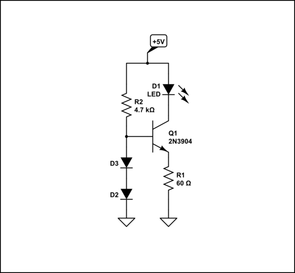
This technique of pinching off forward voltage can actually be used. For example, here's a simple current limiting circuit:

simulate this circuit
D2 and D3 will keep the base voltage at approximately 1.2V. A small base-emitter current will flow, allowing a much larger collector-emitter current to flow which lights the LED. Both the B-E and C-E current will flow trough R1 to ground, causing a voltage drop in R1 which lifts the emitter voltage. When the drop over R1 reaches around 0.6V the B-E will start being pinched off. So current is limited to around 10mA.
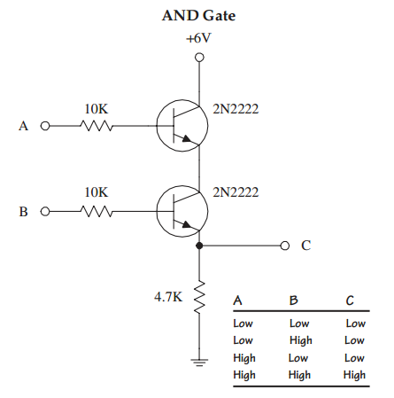
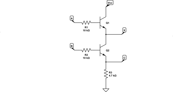
As for your second circuit, it pretty much functions as you said. Applying 6V to the base resistors of both transistors allows base-emitter current to flow in both transistors. This allows collector-emitter current to flow in both transistors and current can flow from the +6V supply to point C.
Apply ground to any of both base resistors and base-emitter current can no longer flow in that transistor and thus no more collector-emitter current.
The 4.7K resistor here is simply a pull-down to keep point C at a low level when any or both transistors are off.

