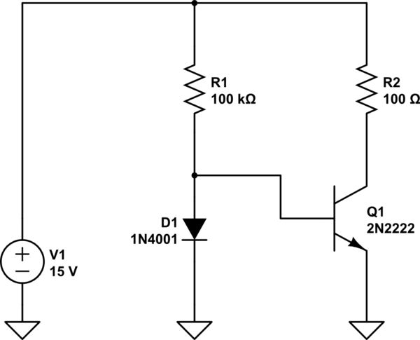
Please help me to calculate the value of resistor R1 so that the current through R2 was 100uA. The only thing I noticed is that the output current is pretty much sensitive to changes of saturation current Is of both diode and transistor.
-
1\$\begingroup\$ This is not how to design a CC unless you assume Vbe and D1 are identical junctions and hFE is fixed. Thus you use fixed R ratios on emitter and collector so hFE is less an effect then 2 diodes or a transistor instead of D1 to sense Re voltage and regulate Vbe. so this is purely academic poor discrete design, but ok if matched parts inside an IC \$\endgroup\$– D.A.S.Commented Sep 22, 2016 at 15:23
-
\$\begingroup\$ If D1 is identical to Vbe junction Rs values then they shared current equally, then Ic=hFE * I(R1)/2.. When matched this is called Current Mirror \$\endgroup\$– D.A.S.Commented Sep 22, 2016 at 15:28
-
\$\begingroup\$ What Tony Stewart said. The coursework must include transistor gain. What is it? \$\endgroup\$– WhatRoughBeastCommented Sep 22, 2016 at 16:01
-
\$\begingroup\$ hfe is 154, but I ran the parameter sweep and the output current doesn't change much with hfe changing \$\endgroup\$– ArchimedesCommented Sep 22, 2016 at 16:04
3 Answers
If you assume that the junctions are the same (patently false, and this dubious assumption must be stated), then the current through R2 ~= current through R1 since \$\beta>>1\$ . You know the voltage at the base of the transistor within a reasonable margin, so you can calculate the current through R1. The value of R2 is not important unless you take 2nd-order effects such as the Early voltage into account. To see how far off the initial assumption is in reality, let's simulate it with a 100K resistor:

simulate this circuit – Schematic created using CircuitLab
The current through R1 is 145uA and the current through R2 is 360uA according to the simulation. So the error is about 2:1 and there's really no point bothering about the 0.3% or whatever due to hFE.
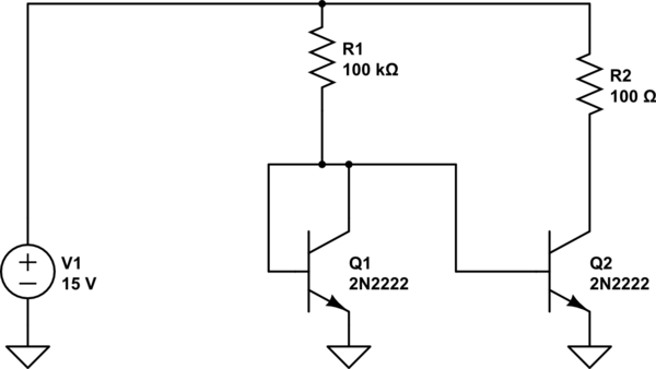
This error originates from the difference in saturation currents of the two junctions and also the ideality factor of the diode junction, which is 1.45 in the above simulation. If I replace the diode with a diode-connected 2N2222, the currents will be much closer:

Now the currents are 145uA and 169ua so the error is only about 15%, but hFE is still an effect of little significance. The error at this point is mostly due to the Early voltage.
Note that you have to use a reasonably accurate transistor model to get reasonably accurate results. In this case Circuitlab (and also the free LTSpice) use good models (Ebers-Moll) with good default parameters and give consistent results showing about 15-20% error.
-
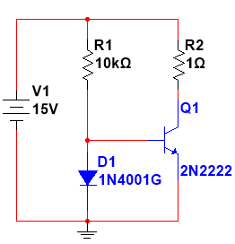
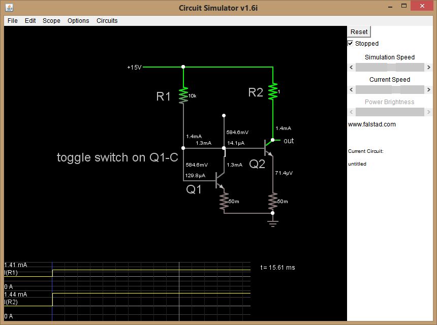
\$\begingroup\$ With Q1-C tied to Q1-B you should get perfect mirroring for high hFE. The error difference I get is only <1% at hFE=100, this goes to zero as hFE increases and Vcc increases. ( So I disagree with your result hFE of Q1 has no effect, also When Q1-C is open, I(R2) will double goo.gl/6nyB27 <=Java simulation ( R1 changed to 10K to reflect question now) \$\endgroup\$– D.A.S.Commented Sep 22, 2016 at 20:00
-
\$\begingroup\$ @TonyStewart What is VAF (Early effect voltage parameter) of your SPICE model? Typically it's 75-100V, which accounts for the 15-20% error since Vce modulates Ic for fixed Vbe with a factor of (1+Vce/Vaf). This parameter is within a sensible range for default 2N2222 models used in both LTSpice and Circuitlab and both give consistent results (15-20% error) which disagree with the simulator (or models) that you are using. The key thing is that 15V is significant compared to 75-100V, and R2 << R1 so Vce is very different on the two transistors. \$\endgroup\$ Commented Sep 22, 2016 at 20:29
-
\$\begingroup\$ If I compute the leakage from Early effect ,Va Va=75V/1mA=75k has no effect on Q1 <0.6V, but at 100uA it is more significant 6% error goo.gl/YiB5T9 \$\endgroup\$– D.A.S.Commented Sep 22, 2016 at 20:53
-
\$\begingroup\$ @TonyStewart It's not "leakage". Ratio of currents due to the Early effect with Vce1 = 0.6 and Vce2 = 14V is: \$\frac{V_{AF}+14}{V_{AF}+0.6}\$, which is 15-20% different. \$\endgroup\$ Commented Sep 22, 2016 at 21:04
-
\$\begingroup\$ in any case these designs have poor V+ sensitivity for Current \$\endgroup\$– D.A.S.Commented Sep 22, 2016 at 21:08
What you have there is a circuit that, when you increase the current through R1, the current through R2 will increase.
However, that's the only thing that can be said about it for certain. The actual ratio of R2 to R1 current is poorly controlled. As you say, it depends on the detail of the diode and transistor base-emitter conduction.
It's easy enough to arrive at a current through R1 to give any R2 current, if you make assumptions about D1 and Q1 parameters, and the temperature. It will be dependent on which model the simulator uses for the transistor. Be aware that this mode is almost never used, well, certainly never trusted in this region, so the models may well be quite inaccurate, as they don't need to be accurate, as nobody would trust them here anyway. If you give an answer based on your simulator, make sure you quote the transistor model, and its parameters, in your answer.
You might well, for the sake of your answer, assume the diode conduction curves for D1 and Q1 are identical if you like, as long as you state the assumption.
To make a proper (robust with temperature, and various device types) current source, place a resistor in series with the diode, and a resistor in series with Q1 emitter. Aim to drop around one volt at the design output current. This will be sufficient to swamp the differences in diode voltage for most 'biassing' purposes, though a precision current source it still isn't.
For 100uA output, put 10k in Q1 emitter. Now you can choose the D1 series resistor to scale the output current if you like. A 100k resistor would result in an output current of 10x I(R1), a 1k resistor of 0.1xI(R1).
-
\$\begingroup\$ I know about the circuit with the resistor, connected to the emitter, it's much easier to calculate, but the problem is that this circuit is actually my university homework, so I can't change it. \$\endgroup\$ Commented Sep 22, 2016 at 15:29
-
\$\begingroup\$ Either change universities or post the full question as it was asked. There's something not right. \$\endgroup\$ Commented Sep 22, 2016 at 16:11
-
\$\begingroup\$ This is the exact circuit and exact question. \$\endgroup\$ Commented Sep 22, 2016 at 16:27
-
\$\begingroup\$ @Archimedes it sounds therefore that you need to make, and state, some judicious assumptions. \$\endgroup\$– Neil_UKCommented Sep 22, 2016 at 16:30
-
\$\begingroup\$ @Archimedes: I understand that the diagram is the original but what you posted starts with "Please help me ..." and this is unlikely to be the exact question. Add it into your original post. \$\endgroup\$ Commented Sep 22, 2016 at 17:20
I(R1) will equal I(R2) when the same transistor is used for the diode within 2% unless Hfe of Q2 is very large (>500) Here simulated with hFE=100 for Q2


