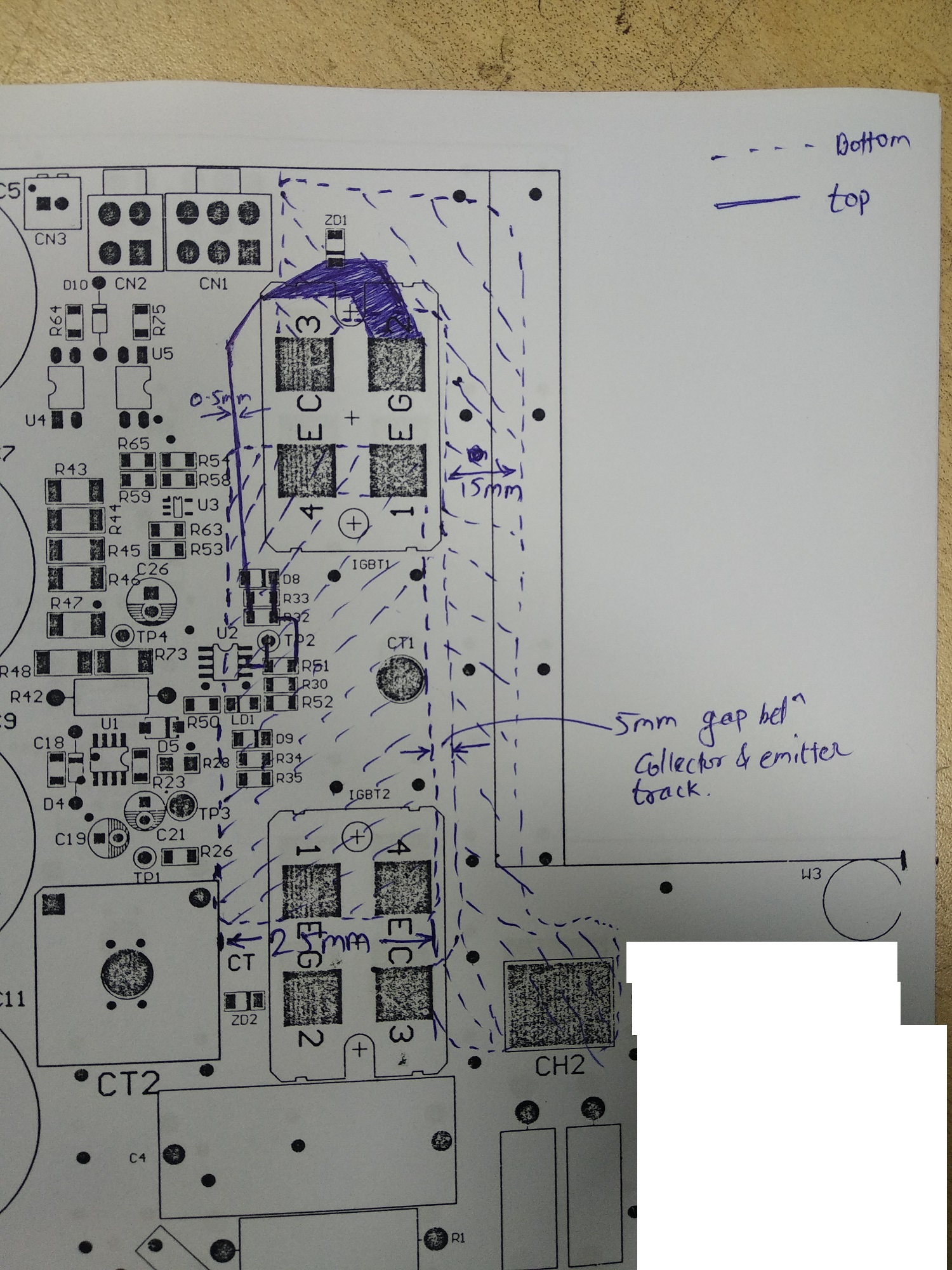
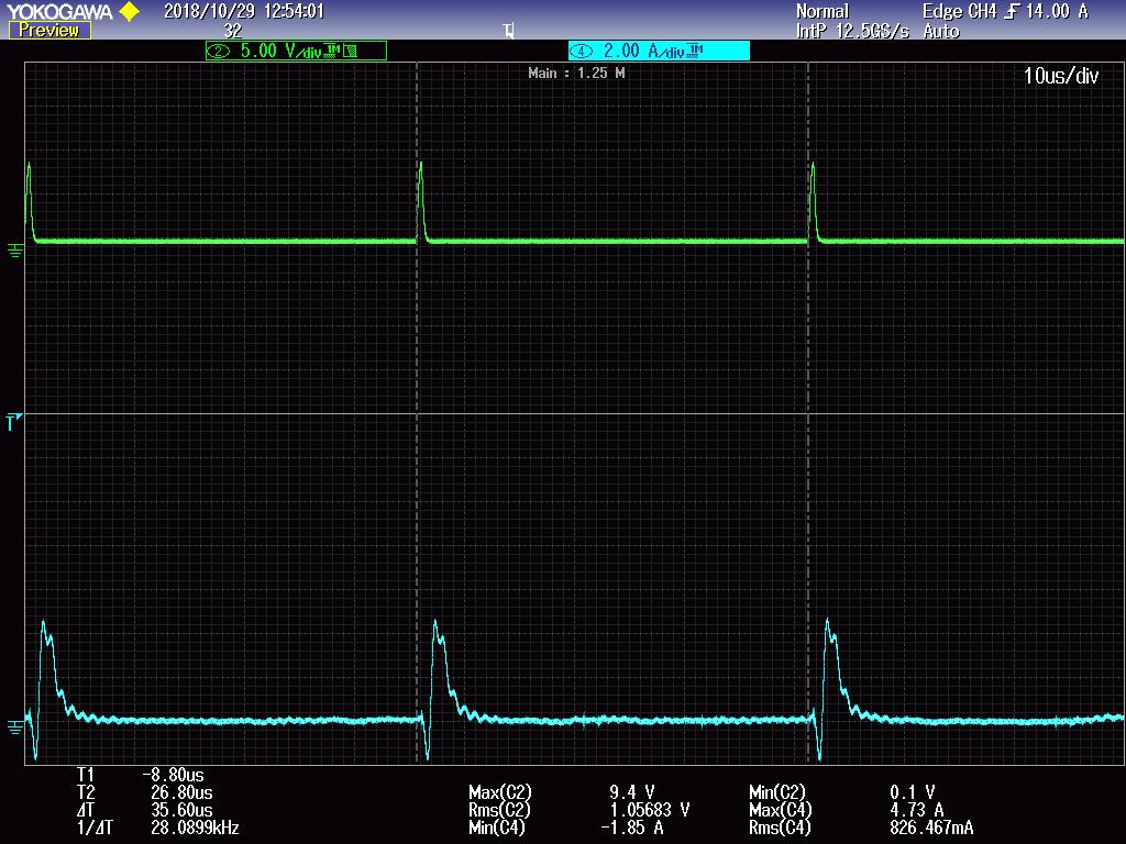
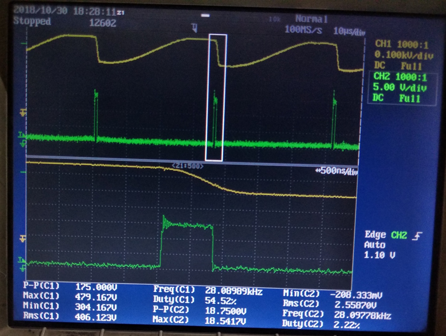
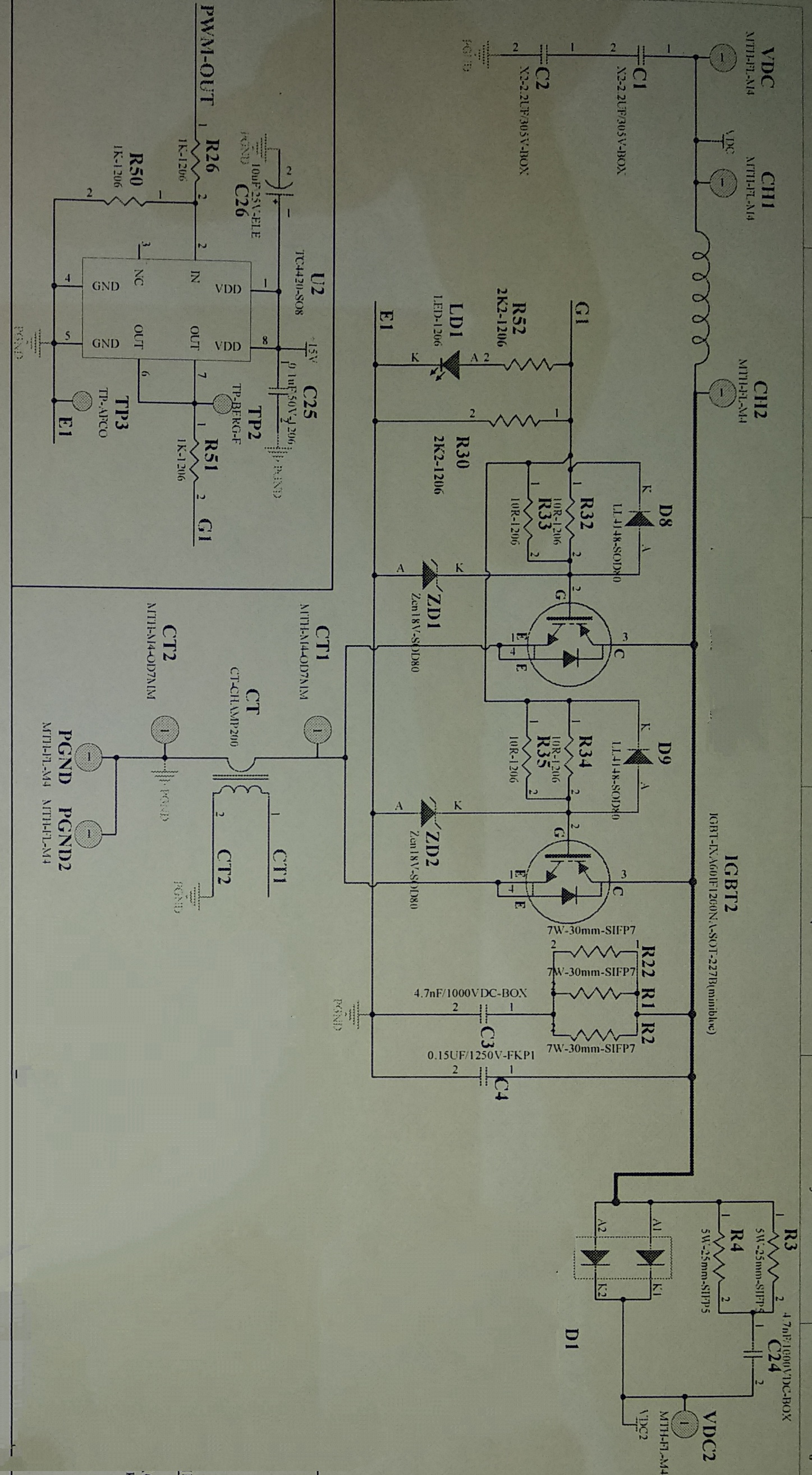
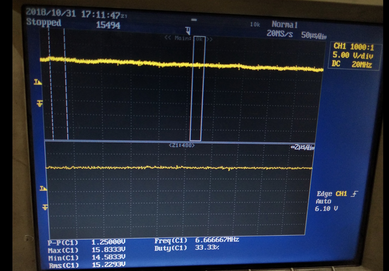
 Here I am applying 3-phase rectified dc to the non-isolated boost converter, the magnitude of applied voltage is 450V and desired o/p voltage is 475V. Switching frequency of PWM is 28k. I am using TC4420 driver IC to drive the IGBT (IKW40N123H3). But when I am starting PWM circuit IGBT's temperature is increasing at a very high rate and this causing igbt failure. I have captured gate to emitter waveform and collector to emitter waveform and I found that collector to emitter waveform is not right. Its voltage is not approaching to zero when GATE PULSE is high. What might be the reason for such a collector-emitter waveform?
\$\begingroup\$
\$\endgroup\$
21
-
2\$\begingroup\$ I have found IGBT's to be very sensitive to ground bounce. Source must have a low resistance ground return to power source. Usually 10 to 12 volts will saturate the IGBT ON. Less than 10 volts but > 3V is in the linear region and it will get HOT! Do you have it mounted to a heatsink? You should. \$\endgroup\$– user105652Commented Oct 31, 2018 at 5:16
-
\$\begingroup\$ Yes, I am using heatsinkand it is also getting very hot. I didn't understood yoursecond sentense (Source must have a low resistance ground return to power source) \$\endgroup\$– vckCommented Oct 31, 2018 at 5:34
-
\$\begingroup\$ @Vick. I mean the IGBT source lead must use heavy gauge wire or wide-thick trace back to power source \$\endgroup\$– user105652Commented Oct 31, 2018 at 6:27
-
1\$\begingroup\$ Show photo of your wiring, including the gate-driver. \$\endgroup\$– analogsystemsrfCommented Oct 31, 2018 at 9:54
-
1\$\begingroup\$ Oh! minibloc. :-( If you add up the delay, rise and fall times of the device, it's about 450 ns, so your ~900 ns on-time will be just about only switching losses. If you move your scope to your Vge pins, you will see the ground jump and all gate impedance on top of that, so I'm not sure you have anything left. Can you float your scope or use diff probe and place local ground at the collector and measure actual gate on one channel and gate driver output on the other? \$\endgroup\$– winnyCommented Nov 1, 2018 at 11:39
|
Show 16 more comments
1 Answer
\$\begingroup\$
\$\endgroup\$
7
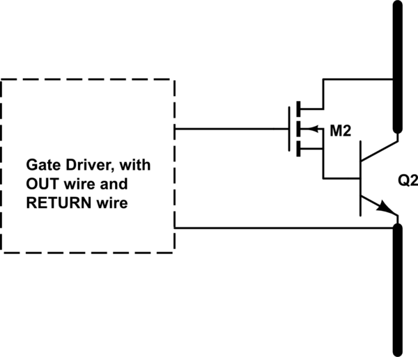
To avoid damage from Ground Bounce, as noted by Sparky256, plan your wiring like this
simulate this circuit – Schematic created using CircuitLab
-
\$\begingroup\$ @winny I have added waveform of driver IC supply during switching. It seems ok. \$\endgroup\$– vckCommented Oct 31, 2018 at 11:32
-
\$\begingroup\$ connection from driver IC to gate-emitter of IGBT is in same manner as shown in your picture. \$\endgroup\$– vckCommented Oct 31, 2018 at 11:37
-
\$\begingroup\$ What about magnetic coupling from the high-slew-rate current into the gate-control loop? Or coupling via electric-fields? How close is the Gate wiring to the collector wiring? \$\endgroup\$ Commented Oct 31, 2018 at 16:28
-
\$\begingroup\$ There is a TRANSFORMER in the emitter. Thus your wiring cannot be as I drew in the answer. \$\endgroup\$ Commented Oct 31, 2018 at 16:29
-
\$\begingroup\$ Gate trace is 5mm apart from collector trace. \$\endgroup\$– vckCommented Nov 1, 2018 at 2:51
