0
\$\begingroup\$

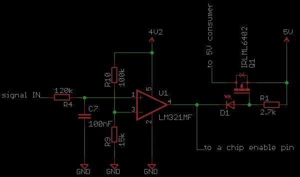
I have the following schematic (extract):
enter image description here

The purpose of this is to enable a pin (chip enable) and to disable the 5V supply ("5V consumer") if the threshold at the signal IN is above a certain threshold (VRef=0.5V). So far so good, the circuit works fine under "normal" circumestances.

The problem is that when I use the PCB with different power supply and input signals (for testing purposes), th op amp does not switch any more. Here are the differences:

  1. power supply:

    • normally: USB(5V) -> battery charger IC -> 4.2V
    • testing: 5V from Raspberry Pi -> battery charger IC -> 4.2V. In this case I noticed that the 5V are actually about 4.8V, but that's still enough. In both cases, no battery is connected so the battery charger is acting as a voltage regulator.
  2. signal IN:

    • normally: analog audio signal with a bias voltage of 1.3V and no more than +/- 0.4V peak-to-peak voltage.
    • testing: 1.3V DC voltage

So when testing, I measured the 1.3V at the signal IN pin and the 0.5V at the VRef pin of the op amp, but it did not switch, i.e. the chip enable pin remained low and the 5V consumer voltage was still enabled.

The total power consumption of the PCB is under 50mA, so it should not be a problem for the Raspberry Pi to power it. The power supply unit is also rated at 1000mA.

Any idea why this happens? Am I overseeing something? Thanks!

UPDATE

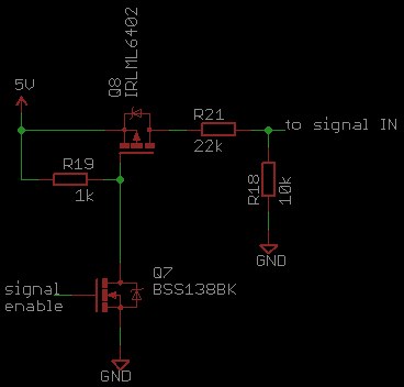
Maybe it's relevant, so I added the circuit which switches the ~1.4V at the signal IN pin:
enter image description here

One thing I noticed: while sweeping the input signal ("signal IN") from 0V to about 2V, I noticed that the op amp does switch above the threshold of about 0.55V, but the output voltage jumps from about -15mV (input under 0.55V) to only 60mV (input over 0.55V).

UPDATE 2

I disconnected the output of the op amp (no load) and now it does not switch any more at all (using the testing method). The output remains low.

I also measured the output of the op amp with an oscilloscope (both with and without load) and it does not switch fast high and low (so it averages to 60mV), as Spehro Pefhany suggested. The voltages are pretty clean, i.e. no spikes or large AC variations.

UPDATE 3

In the last update I said that the op amp does not switch without a load. That was a mistake from my part: it still does switch, but the ON-voltage is at about 30mV.

UPDATE 4

If I power the board (first schematic) normally (5V from USB) and use the Raspberry only to switch the signal (second schematic), the op amp switches correctly! So I tend to think that there is a problem in my power supply. I power the board with the Raspberry very similar as I switch the signal IN (second schematic), except without the R18 and R21 (so I basically feed-through the 5V). The 5V (at Q8) are coming directly from the Raspberry pin header.

\$\endgroup\$
7
  • 1
    \$\begingroup\$ It really sounds like there's something else wrong with your test setup, such as a missing ground connection. Check everything carefully. \$\endgroup\$
    – Dave Tweed
    Commented Jun 17, 2014 at 12:08
  • \$\begingroup\$ Other tests on the PCB work fine, so it's hard to believe that the ground connection is missing. I triple-check everything but still couldn't find any error. \$\endgroup\$ Commented Jun 17, 2014 at 13:38
  • \$\begingroup\$ Just to clarify what you've done there, the first schematic has a low-pass filter at the op-amp input, right? It obviously looks to be so, I am just wanting to ensure that is what the purpose is. In the second schematic, what is the purpose of R21 and R18 - just a divider for the output? Are you toggling Signal Enable? I am still getting accustomed to reading schematics and understanding intent. \$\endgroup\$
    – sherrellbc
    Commented Jun 27, 2014 at 14:50
  • \$\begingroup\$ And also, 5V Consumer appears to be floating when not switched through the FET. Do you have some pull-down resistors no shown? \$\endgroup\$
    – sherrellbc
    Commented Jun 27, 2014 at 14:55
  • \$\begingroup\$ @sherrellbc Yes, it's a low pass filter. Like I said, it's an audio signal with bias voltage at the input, and I'm only interested in the bias voltage there. Also correct: the R21 and R18 divide the 5V input voltage to about 1.3V. And lastly: the schematics is not complete, so don't worry about that floating line ;) \$\endgroup\$ Commented Jun 27, 2014 at 16:19

4 Answers 4

0
\$\begingroup\$

What you describe SHOULD work, so it seems you may be just crossing over a limiting boundary when you change modes. Try it with NO load on the op-amp. If that still doesn't work then circuit is not as you believe OR opamp is damaged.

LM321 data sheet

Presumably the chip enable pin does not provide a massive pullup? Or does it? Try it with nothing connectd to LM321 output pin.

Things to look at include:

Supply voltage. 3V in datasheet so 4V2 or 5V OK.

Max Vcommon_mode = Vdd - 1.5V or 2V depending on conditions. In either case you SHOULD be well below that.

Massive output pullup - see above. The LM321 and LM314 (quad big brother) data sheets provide sink currents at high supply voltages but not at low voltage. IF these decrease with supply voltage you may be below the 1 to 2 mA needed by the LED etc.

\$\endgroup\$
1
  • \$\begingroup\$ The op amp is not damaged because the PCB still works if I operate it normally. There is a measurable difference in voltage at the op amp output pin (in testing mode): if signal IN is low, the output is about 0.003V and if it's high (1.3V), the output is 0.068V. \$\endgroup\$ Commented Jun 17, 2014 at 14:07
0
\$\begingroup\$

The output impedance of the RPi might be high enough to give you some negative (or positive) feedback through the VCC line to the op-amp.

Sweep the input beyond your normal ranges (but within the allowable maximums from the datasheet) while watching the output of the op-amp:

  • If it moves with the input then it's acting like an amplifier instead of a comparator.
  • If it switches, but at a much higher voltage, you have hysteresis due to positive feedback.
\$\endgroup\$
1
  • \$\begingroup\$ See my first update. The op amp does switch, but to only 60mV, not VDD. \$\endgroup\$ Commented Jun 26, 2014 at 10:52
0
\$\begingroup\$

The ~60mV differential implies that that "chip enable" input is actually an output and is effectively shorting the LM321 output to ground. Or something like that. Another possibility is that it is very briefly switching above ground and back again and it averages to ~60mV. If you don't have access to an oscilloscope, one way to check that is to connect another LED + resistor from the output to ground. You wouldn't be able to see the slight reduction in brightness of D1 if the output was switching above ground with a low duty cycle, but you would be able to see the difference between dark and dimly lit for an LED connected from the output to ground (with a few hundred ohms in series).

Using the LED to level shift the output a bit is clever, and should work, but your system should have some kind of UVLO lockout protection so if the 4.2V battery drops too low, the battery will be protected for one thing, and secondly so the MOSFET won't damage or unsolder itself when the gate voltage becomes insufficient to fully turn it on. Maybe you've got that elsewhere.

\$\endgroup\$
0
\$\begingroup\$

I found the problem: it was a mean, little shortcut to GND at the output of the op amp. So I was looking in the wrong place at first. The circuit as-is works fine.

Thanks for all the answers!

\$\endgroup\$

Your Answer

By clicking “Post Your Answer”, you agree to our terms of service and acknowledge you have read our privacy policy.

Not the answer you're looking for? Browse other questions tagged or ask your own question.