20
\$\begingroup\$

I am very familiar with the operation of bootstrap drivers on MOSFET driver ICs for switching an N-channel high-side MOSFET. The basic operation is covered exhaustively on this site and others.

What I don't understand is the high-side driver circuitry itself. Since a good driver pushes and pulls large amounts of current, it makes sense that another pair of transistors exist within the IC to drive the VH pin high or low. Several datasheets I've looked at seem to indicate they use a P-channel/N-channel pair (or PNP/NPN). Taking away the construct of the IC chip, I imagine the circuit looks something like this:

schematic

simulate this circuit – Schematic created using CircuitLab

It seems that we've just introduced a recursion problem. Assuming the node marked as "floating" can be any arbitrarily high voltage, how are M3 and M4 driven that doesn't need yet another driver to drive the driver (and so on and on)? This is also assuming the high-side driver is ultimately controlled by a logic-level signal of some kind.

In other words, given an arbitrarily high floating voltage, how is the push-pull drive of M3 and M4 activated by a logic-level signal that originates from off the chip?

Point of clarification: The specific question I'm asking has only to do with activating the high-side push-pull bootstrap drive with a logic-level signal. When the high-side voltage is relatively low, I recognize this is trivial. But as soon as the voltages exceed typical Vds and Vgs ratings on transistors, this becomes harder to do. I would expect some kind of isolation circuitry to be involved. Exactly what that circuitry looks like is my question.

I recognize that if M4 is a P-channel FET (or PNP), another bootstrap circuit is not necessary. But I'm having trouble conceiving of a circuit that will generate the proper Vgs's for both M4 and M3 as the external transistors are switched back and forth.

Here are screen captures from two different datasheets that show a similar circuit to what I drew above. Neither go into any detail about the "black-box" driver circuitry.

From the MIC4102YM:
enter image description here

And the FAN7380:
enter image description here

\$\endgroup\$
7
  • \$\begingroup\$ Dan, since you wrote that you've looked at several datasheets, could you post the links to them? That would provide a nice context. \$\endgroup\$ Commented Nov 4, 2014 at 0:10
  • \$\begingroup\$ Sure, I'll update the question with some examples I found. \$\endgroup\$
    – Dan Laks
    Commented Nov 4, 2014 at 2:26
  • \$\begingroup\$ Dan, earlier in this answer I have detailed the operation of a bootstrap gate driver like FAN7380. \$\endgroup\$ Commented Nov 4, 2014 at 3:17
  • 2
    \$\begingroup\$ Nick, I actually found that answer earlier before posting my question (although the fact I used the same image from the FAN7380 datasheet is a coincidence). I'm fairly comfortable with using a driver IC with a bootstrap gate drive. The specific question I'm asking is what the gate drive circuit actually looks like. The box marked as just "driver" in the image. Basically, specific details about step 4 of your answer to that earlier question. \$\endgroup\$
    – Dan Laks
    Commented Nov 4, 2014 at 3:27
  • 1
    \$\begingroup\$ Right, the push-pull pair is what I figured in my question. I'm still missing something though. How does the push-pull drive activate for arbitrarily high floating voltages? That's the crux of my question, I suppose. \$\endgroup\$
    – Dan Laks
    Commented Nov 4, 2014 at 3:51

2 Answers 2

19
\$\begingroup\$

schematic

simulate this circuit – Schematic created using CircuitLab

Note 1: The input voltages are only \$V_{cc}\$ and \$V_\text{High Voltage}\$. You don't apply anything at the \$V_{BS}\$ node. It is only for representation.
Note 2: Notice that there are two different type of grounds. Those grounds must not be directly connected to each other.

You must drive the MOSFET between its gate and source terminals. Since the source terminal voltage of a high side MOSFET will be floating, you need a separate voltage supply (VBS: \$V_\text{Boot Strap}\$) for the gate drive circuit.

In the schematic below, VCC is the voltage source of the rest of the circuit. When the MOSFET is off, ground of the boot strap circuit is connected to the circuit ground, thus C1 and C2 charge up to the level of Vcc. When the input signal arrives to turn the MOSFET on, ground of the gate drive circuit rises up to the drain voltage of the MOSFET. The D1 diode will block this high voltage, so the C1 and C2 will supply the driving circuit during the on-time. Once the MOSFET is off again, C1 and C2 replenish their lost charges from VCC.

Design criteria:

  • RB must be chosen as low as possible that will not damage D1.
  • Capacity of C2 must be chosen enough to supply the driving circuit during the longest on-time.
  • Reverse voltage rating of D1 must be above \$V_\text{High Voltage} - V_\text{CC}\$.

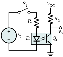
The input signal must be isolated from the boot-strap circuit. Some possible isolaters are:

Optocoupler

enter image description here

Optocoupler is the most basic method for isolation. They are very cheap compared to other methods. The cheap ones have propagation delay times down to 3\$\mu\$s. The ones with less than 1\$\mu\$s propagation delay are as expensive as isolated gate drivers though.

Pulse Transformer

enter image description here

Pulse transformer is a spacial type of transformer for transferring rectangular pulses. They have less number of turns in order to avoid parasitic capacitance and inductance and larger cores for compensating loss of inductance due to reduced number of turns. They are much faster than optocouplers. Delay times are less than 100ns in general. The image above is for illustration only. In practice, the current they can provide is not enough for driving a MOSFET fast; so they need additional circuitry in practice.

Isolated Gate Driver

enter image description here

Isolated gate driving is a relatively new technology. All the complexity of gate driving is encapsulated in one single chip. They are as fast as pulse transformers, yet they can provide a few amperes of peak gate current. Some products also contain on-chip isolated DC-DC converters, so they don't even need boot-strapping. However, all these super features come with a cost.

\$\endgroup\$
5
  • \$\begingroup\$ hkBattousai, thank you for taking the time to write an answer. If you expand on the last three bullet points (that address the question I asked) and remove the details about the basics of bootstrap drivers (that I mention in the first paragraph of my question that I'm already familiar with), you'll have my +1. The opto-isolator circuit is great and I was hoping to get answers that focus entirely on that part of the driver instead of the general basics of how bootstraps work. \$\endgroup\$
    – Dan Laks
    Commented Nov 4, 2014 at 16:19
  • 2
    \$\begingroup\$ I think we shouldn't remove details of boot-strapping. Other users may benefit from it. \$\endgroup\$ Commented Nov 4, 2014 at 17:29
  • \$\begingroup\$ I'm fine with that, as long as the answer is now focused mostly on the specific question (as it is now). Thank you and +1. \$\endgroup\$
    – Dan Laks
    Commented Nov 4, 2014 at 17:35
  • \$\begingroup\$ Hi, I see the last image you provided is very similar to the schematic of the ADuM3220 gate driver. My question is if this requires bootstrapping to power the high-side MOSFET? IF not, do you have an example of a product with an on-chip isolated dc-dc converter? Thanks \$\endgroup\$
    – rrz0
    Commented Apr 9, 2018 at 16:38
  • 1
    \$\begingroup\$ @Rrz0 In this table, for a product listed in a row, if the string in the column "Isopower Enabled" is "Yes", then it has internal DC-DC power supply. \$\endgroup\$ Commented Apr 10, 2018 at 7:35
5
\$\begingroup\$

Um, the IC has internal "level-shift" circuit.

enter image description here

And the level shift circuit maybe like this, this is similar with FAN7380:

enter image description here

The two NMOS before Pulse Filter is relative to the true ground, and the difference signal it routed to Pulse Filter. After Pulse Filter, the ground is floating on \$V_{SRC}\$, and the supply is \$V_{BST}\$.

And below is IR2110's block diagram (From International Rectifier AN978-b):

enter image description here

\$\endgroup\$
2
  • \$\begingroup\$ Yes, chips have a level shifter of some kind. How it implements the level shifter for an arbitrarily high voltage is the specific question I'm asking. \$\endgroup\$
    – Dan Laks
    Commented Nov 4, 2014 at 16:24
  • 1
    \$\begingroup\$ I've edited my question to add an extra paragraph to clarify. \$\endgroup\$
    – Dan Laks
    Commented Nov 4, 2014 at 16:34

Your Answer

By clicking “Post Your Answer”, you agree to our terms of service and acknowledge you have read our privacy policy.

Not the answer you're looking for? Browse other questions tagged or ask your own question.