6
\$\begingroup\$

I just received my DigiKey order of some Atmel ATTiny4 MCU's from DigiKey. I wanted to tinker with one of the smallest MCU's I could find, and this was one of them.

It is, in fact, so small because it is wafer level chip scale packaging (WLCSP), described here. This image from that document indicates scale.
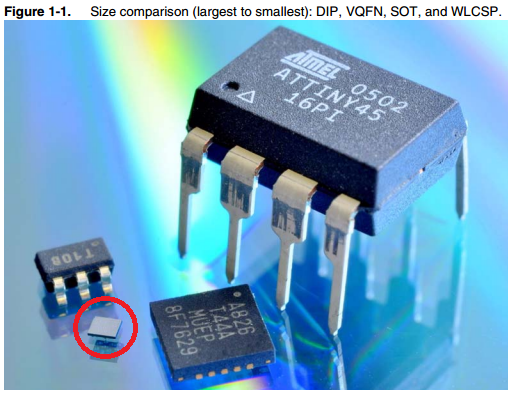
enter image description here

This question may be very naive, but how do I "hobby" with a chip this size?

I cannot directly plug it in to a breadboard. (Unless there is some socket I can buy that I am unaware of?) Programming the chip is the next step, but I do not know what hardware I need to interface with my PC. There are plenty of tutorials out there on the web that show to program a DIP (with an Arduino, for example). I cannot, however, find any information on how to program these tiny chips.

Is this even possible for someone (me) tinkering out his apartment? Or are these chip sizes primarily sold to manufactures of electronic devices with automated systems for integrating these chips?

Note: I am not sure how to tag this question. Feel free to edit.

\$\endgroup\$
3
  • \$\begingroup\$ The linked document pretty much tells you. Just treat it like a BGA ;-) I'd want to get some experience with 0.8mm pitch BGAs before moving on to 0.4mm pitch. Doesn't look easy... \$\endgroup\$
    – user16324
    Commented Dec 15, 2014 at 15:41
  • 1
    \$\begingroup\$ Just to make it clear, all the Atmel chips shown in that photo will have the same silicon die, just varying amounts of black epoxy packaging. \$\endgroup\$
    – pjc50
    Commented Dec 16, 2014 at 0:12
  • 1
    \$\begingroup\$ The same size die, for a liberal definition of "same"; those are actually 4 different models. \$\endgroup\$ Commented Dec 16, 2014 at 2:36

6 Answers 6

6
\$\begingroup\$

I'm sorry, but you've got no chance.

It's basically an ultra-small BGA - you need to reflow it properly onto a PCB, and at that scale it's going to be very very hard to both get and keep the alignment properly (and even generate the PCB in the first place). Better to stick to DIP.

As for programming them - you route the programming pins out to a header on your PCB and connect a normal AVR ICSP of some form into it.

\$\endgroup\$
8
\$\begingroup\$

It's not impossible to solder them yourselves, contrary to the impression other people are giving. You could even solder them by hand! http://hackaday.com/2013/07/03/hand-soldering-bga-wafer-chips/

I'd also recommend looking at the skillet technique from SparkFun: https://www.sparkfun.com/tutorials/59

\$\endgroup\$
7
\$\begingroup\$

It's possible you could reflow this tiny BGA onto a gold-plated PCB (flux only, no paste) with a toaster oven approach, but your yield may not be 100% on the first try. It has to be placed within 0.1mm or so (they say +/-0.03mm for production) so a microscope would be a good idea unless your eyes are a lot better than mine.

There's not a lot of advantage in making a breakout board for such a tiny chip. If you really need to break it out to a breadboard, you can just use a similar chip in a larger package (such as a DIP). Programming has little to do with the package, it will be the same kind of ISP serial programming with a header or pogo pins as you'd do with any other similar chip. Other than size and thermal characteristics the package doesn't affect much.

The board will look about the same in EDA software on your computer screen as any other board (when you zoom in), the problems will start with getting the board manufactured to the right specifications (the cheap PCB suppliers will probably not be good enough for the fine features) and especially with actually populating the BGA part.

\$\endgroup\$
4
\$\begingroup\$

Presumably the chip scale package that you purchased is in a part family that has the same part in other types of packages. That said, the programming of the part follows the same procedure and requires the same type of programming adapter as the same part type in bigger leaded packages.

Chip scale packages are made to be direct attached via surface mount techniques right onto circuit board that have the correct pad footprint in place to accept the part.

The only way you can hope to "hobby" with these parts is to do one of the following:

  1. Make a circuit board.
  2. Try to find a suitable breakout board.
  3. Purchase the type of package that can be worked with.

For the first two you would still have to deal with how to get the chip scale package attached to the circuit board. You cannot attach these using a soldering iron in your apartment.

So in conclusion go back and buy the DIP packaged part so you can use it on your protoboard. Then if your "hobby" activity leads to some type of gadget design that you eventually want to package up on a circuit board and have it be as small as possible you may be able to use your chip scale package.

\$\endgroup\$
2
\$\begingroup\$

Test lead wire - the good, really flexible stuff - is typically made up of dozens of strands of 40awg wire.

If you take some of these strands, mount the chip upside down, and using a very fine tip soldering iron you could conceivably dead bug mount these chips.

That largely defeats the purpose of using such a small chip though. Prototype your device with the larger chips, then design a pcb and mount it using surface mount techniques for the final product.

\$\endgroup\$
1
1
\$\begingroup\$

Either

  1. Have them programmed by the distributor. Good for production or if you have a working bootloader. or
  2. Bring out the programming pins to a header.
\$\endgroup\$

Your Answer

By clicking “Post Your Answer”, you agree to our terms of service and acknowledge you have read our privacy policy.

Not the answer you're looking for? Browse other questions tagged or ask your own question.