0
\$\begingroup\$

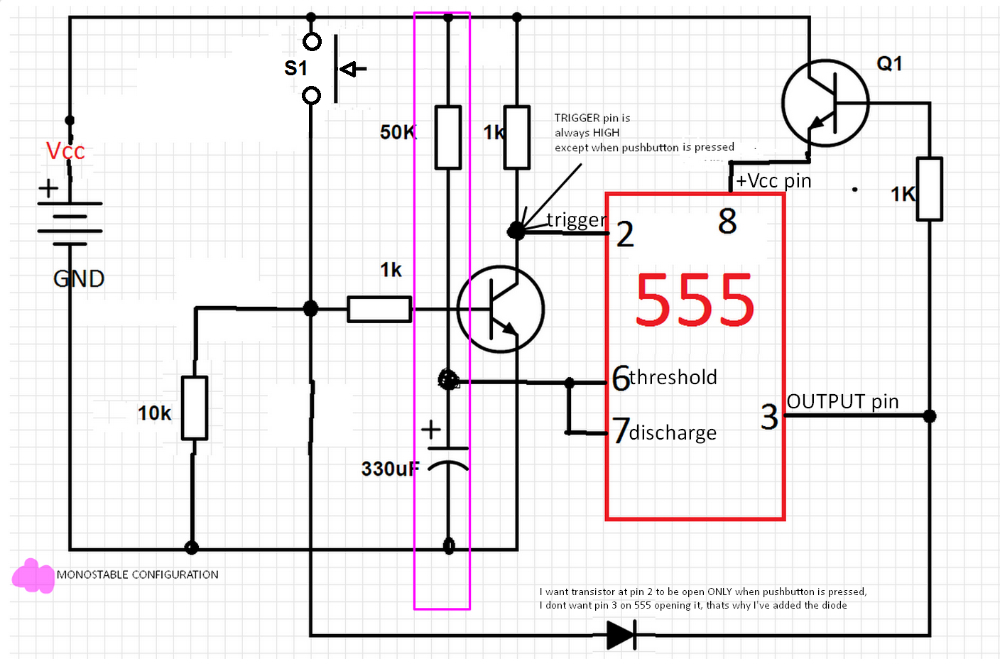
i had idea for a circuit with 555 and here is the IDEA:

circuit is stationary somewhere, it is in "passive state" meaning its drawing no current from battery and pin 3 is set low, then someone comes by, presses the button and LED turns on, after 15 seconds LED turns off and circuit continues to draw no current and remains in this "passive state" untill next button press

QUESTION: this circuit doesn't work, and im wondering where did I make a mistake?

LINK: http://prntscr.com/5u1be2

enter image description here

PS: imagine LED connected to pin 3

\$\endgroup\$
4
  • \$\begingroup\$ Please explain more, the way the circuit needs to work is not clear enough. \$\endgroup\$
    – Triak
    Commented Jan 18, 2015 at 16:24
  • \$\begingroup\$ I edited the text is it more clear now? \$\endgroup\$ Commented Jan 18, 2015 at 16:50
  • \$\begingroup\$ Where is the question? \$\endgroup\$
    – caveman
    Commented Jan 18, 2015 at 16:57
  • \$\begingroup\$ my bad, i've added it. This circuit doesnt work for some reason, im wondering what that reason is. \$\endgroup\$ Commented Jan 18, 2015 at 16:58

3 Answers 3

4
\$\begingroup\$

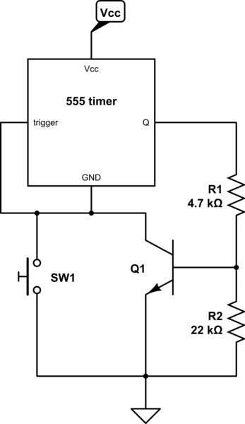
Something like this will work. Timing and bypass components and load omitted for clarity.
schematic

simulate this circuit – Schematic created using CircuitLab

When the output goes high, it turns on Q1 through R1, which turns on Q2 via R2. R2 should be low enough that Q2 stays reliably saturated with the highest load on the 555, plus the 555 supply current. R3 prevents leakage in Q1 from being amplified by Q2, so the total leakage in the passive state is merely the leakage in Q1 + Q2 (probably in the 10's of nA at room temperature), rather than tens or hundreds of times higher.

Edit: Expanding on the leakage- suppose the leakage of Q1 is 20nA, and gain of Q2 at 20nA is 40. All the leakage current from Q1 flows into the base of Q2. Then the collector current of Q2 will be 40 * 20nA = 800nA plus another 20nA for its leakage, so a total of 840nA. That's without R3.

Now add R3- the voltage across R3 will be 20nA * 20K = 400uV. That means virtually all the current will flow through the resistor and not the base (since the base-emitter junction doesn't really start to conduct until the voltage across it reaches hundreds of mV) so the leakage of Q2 is just the minimum 20nA, for a total of 40nA (21x better performance for a single resistor).

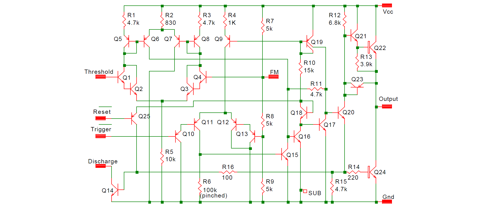
Edit2: Further to discussing why use this circuit as opposed to lifting the GND pin, here's the schematic of the original 555. It should be reliable as it is from the designer's (Hans Camenzind, RIP) book Designing Analog Chips.
enter image description here

Edit 2:

In order for the trigger to work properly in conjunction with the above-discussed power switching scheme- consider the below schematic. R6 may not be necessary.
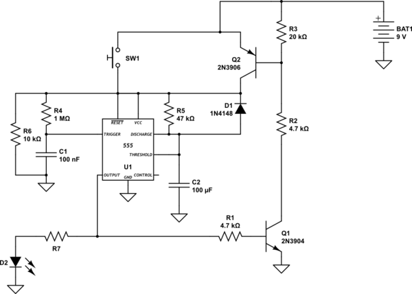
schematic

simulate this circuit

\$\endgroup\$
13
  • \$\begingroup\$ is there any reason for my circuit to not work (not op here)? \$\endgroup\$ Commented Jan 18, 2015 at 18:18
  • \$\begingroup\$ @VladimirCravero Yes, I don't think the 555 output will go below GND more than one diode drop. \$\endgroup\$ Commented Jan 18, 2015 at 18:26
  • \$\begingroup\$ I'm missing a pull down resistor of course. Thanks. \$\endgroup\$ Commented Jan 18, 2015 at 18:27
  • 1
    \$\begingroup\$ @VladimirCravero Even with a pull-down I don't think it will- there is a parasitic diode from the output to GND that's normally reverse-biased. \$\endgroup\$ Commented Jan 18, 2015 at 18:39
  • \$\begingroup\$ You told me the purpose of R3 on the schematics, but I dont understand how does it prevent leakage. as far as I know all It would do is instead of all current flowing thru Q2, some would also go throught R3, thus Q2 being less conductive. What am i missing \$\endgroup\$ Commented Jan 18, 2015 at 18:42
1
\$\begingroup\$

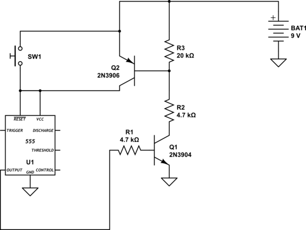
As Olin pointed out there's no way you can control a circuit power with an emitter follower from one of the circuit outputs itself, unless your circuit can provide an output voltage higher than the input, which is possible but is not the 555 case.

There actually is a way to achieve your goal:

schematic

simulate this circuit – Schematic created using CircuitLab

When you press the button the circuit is powered, Q goes high and the bjt turns on, keeping the circuit powered when the button is released. After the time set by the 555 subcircuit Q goes low and turns off the bjt.

There are two things you should notice:

Since \$V_{CE}=0\$ the bjt might not turn on properly, you might try to include a resistor in series with the pushbutton (aim for some 2~200mV drop), or you need to replace the bjt with a relay.

Note that I connected the trigger to gnd through the pushbutton. Any other pin of that subcircuit that must be tied to gnd must be connected through the pushbutton, or your 555 might get some power from the protection diodes.

\$\endgroup\$
11
  • \$\begingroup\$ im no expert but wouldn't i have to place a big pull up resistor from Vcc to GND pin because otherwise I'd make Trigger and GND pin "floating"? \$\endgroup\$ Commented Jan 18, 2015 at 18:20
  • \$\begingroup\$ leaving them floating is precisley what you want to do since you want to turn off the IC. \$\endgroup\$ Commented Jan 18, 2015 at 18:24
  • \$\begingroup\$ but why does my "design" not work ive spent hours on trying to figure it out \$\endgroup\$ Commented Jan 18, 2015 at 18:32
  • \$\begingroup\$ As Olin said and as I quoted: you can't control a circuit power with an emitter follower. My solution, as well as Spehro, uses transistor(s) in common emitter configuration, and that can work. \$\endgroup\$ Commented Jan 18, 2015 at 18:35
  • 1
    \$\begingroup\$ There is an isolation diffusion that will become forward biased, similar to a "protection diode" in a CMOS chip. Even if you don't believe me, a quick look at the schematic will tell you that the best case is a 4.7K series with 220 ohms series with a forward-biased Vce junction from output (negative) to GND. That will turn the transistor on easily, even with R2. \$\endgroup\$ Commented Jan 18, 2015 at 18:56
1
\$\begingroup\$

I looked at it only briefly since the 555 timer pins were just numbers without explanation. However, 2 things jumped out:

  1. The pushbutton is permanently shorted. That of course would cause the circuit to ignore any pushbutton state changes.

  2. It looks like you might be trying to power up the chip with a NPN emitter follower. That can't work. The output voltage of the emitter follower will always be less than what you are driving the base with. Since the chip can't produce a voltage higher than its own power voltage, you can't drive that power voltage from a output pin thru a emitter follower.

\$\endgroup\$
6
  • \$\begingroup\$ 1. Pushbutton doesnt short out anywhere, only connections are at the points where there is a BLACK DOT present, unless i am missing something here ... 2) output pin ( pin 3 ) is opening NPN transistor, which is then connecting VCC and power supply pin on IC ( that is pin 8) \$\endgroup\$ Commented Jan 18, 2015 at 17:12
  • 2
    \$\begingroup\$ @Not: I just checked again, and the schematic clearly shows the pushbutton shorted. \$\endgroup\$ Commented Jan 18, 2015 at 17:13
  • \$\begingroup\$ here is the current flow prntscr.com/5u19so DOTS represent connections \$\endgroup\$ Commented Jan 18, 2015 at 17:16
  • \$\begingroup\$ @Not_Important: Olin is right. I've edited your drawing to show the correct use of the switch symbol, but without addressing the rest of the circuit's errors. \$\endgroup\$
    – EM Fields
    Commented Jan 18, 2015 at 21:02
  • \$\begingroup\$ what he ment to say was pushbutton was normaly closed instead of being normaly open? \$\endgroup\$ Commented Jan 18, 2015 at 21:34

Your Answer

By clicking “Post Your Answer”, you agree to our terms of service and acknowledge you have read our privacy policy.

Not the answer you're looking for? Browse other questions tagged or ask your own question.