1
\$\begingroup\$

Semtech is providing a reference design concerning the SX1272 chip:

SX1272 modules: SX1272MB1DCS - 868 MHz - Combined RFI and RFO, switchless (Ref design only)

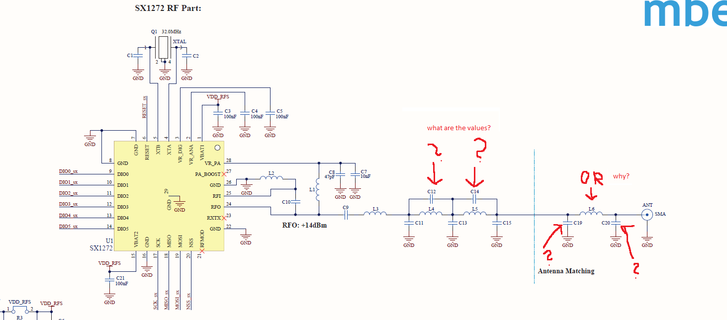
I can't find the values of C12, C14, C19 and C20 capacitors in the bill of materials. These should be somehow calculated or what?

Moreover, there are 0R resistors, what are they for?

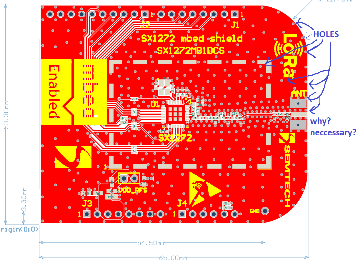
And what are the holes in PCB for? Are they necessary?

Sorry, if this question is trivial. I never designed antenna's part of PCB.

enter image description here

enter image description here

\$\endgroup\$
4
  • 1
    \$\begingroup\$ making pictures of the important parts of the gerbers would make it a lot easier for us to see what you're talking about without having to fire up a gerber viewer. \$\endgroup\$
    – The Photon
    Commented Apr 12, 2016 at 23:39
  • \$\begingroup\$ I'm talking about schematic in PDF file. I will attach an image. \$\endgroup\$
    – Defozo
    Commented Apr 12, 2016 at 23:40
  • \$\begingroup\$ Those are load options -- they are not all supposed to be present at the same time. As for 0R resistors, they are often used to provide a place to tweak the value, or to remove it and insert measurement equipment. By placing these there now in schematic, the pads are there in layout for you to use if necessary. \$\endgroup\$ Commented Apr 12, 2016 at 23:45
  • \$\begingroup\$ Load options? Could you explain? \$\endgroup\$
    – Defozo
    Commented Apr 12, 2016 at 23:49

2 Answers 2

6
\$\begingroup\$

I can't find the values of C12, C14, C19 and C20 capacitors in the bill of materials. These should be somehow calculated or what?

This is the question I'm least sure about. Maybe these are intended to be not loaded. This would be the case if they determined they only needed a low-pass filter instead of a band-pass filter after designing and testing the board.

Moreover, there are 0R resistors, what are they for?

If L6 is a 0-ohm resistor, it's to connect the two nets together without adding another inductor.

R3 is a 0-ohm resistor to allow you to remove it and test the current consumption of the circuit by connecting an ammeter between the nearby test points.

And what are the holes in PCB for? Are they necessary?

They are called stitching vias. They are to keep the ground net at the same potential on all the layers of the board. This can help avoid, say, the ground planes resonating and disturbing the circuit performance, or acting as an antenna and emitting rf.

I'd say the number of stitching vias is overkill for an 870 MHz circuit. You could probably get away with placing stitching vias only every 10 mm or so (even every 35 mm, to place them at 1/10-wavelength separation) without any degradation in performance. But for a high-quality rf design, I wouldn't eliminate them altogether.

\$\endgroup\$
0
\$\begingroup\$

The 0R resistor and the two unlabeled capacitors near "antenna matching" are an empty "pi network". They can be stuffed with two real capacitors and an inductor to adjust the transmission line impedance to match a given antenna. To start with leave the capacitors unstuffed (that's why they don't appear on the BOM).

See also http://www.edn.com/electronics-blogs/living-analog/4418401/Pi-Network-and--Dipping-the-Final-

Now watch out here: because you're messing with the antenna, if you sell this as a product in the USA you must go through full, not modular, FCC approval. The cost difference between full and modular is 10x or 20x.

\$\endgroup\$

Your Answer

By clicking “Post Your Answer”, you agree to our terms of service and acknowledge you have read our privacy policy.

Not the answer you're looking for? Browse other questions tagged or ask your own question.