2
\$\begingroup\$

I've designed a custom PCB which uses the ESP32-WROOM-32 module. I'm using arduino to help validate the board, and I am able to run very simple programs on it successfully (ex. serial echo, Blink, etc...)

Where I'm having trouble is running any Wifi programs on it. For example, when I load the Wifi Scan example program, I receive the following output.

rst:0x1 (POWERON_RESET),boot:0x13 (SPI_FAST_FLASH_BOOT)
configsip: 0, SPIWP:0xee
clk_drv:0x00,q_drv:0x00,d_drv:0x00,cs0_drv:0x00,hd_drv:0x00,wp_drv:0x00
mode:DIO, clock div:2
load:0x3fff0018,len:4
load:0x3fff001c,len:1216
ho 0 tail 12 room 4
load:0x40078000,len:10864
load:0x40080400,len:6404
entry 0x400806b8
[W][esp32-hal-psram.c:30] psramInit(): PSRAM init failed!
[D][WiFiGeneric.cpp:332] _eventCallback(): Event: 0 - WIFI_READY
[D][WiFiGeneric.cpp:332] _eventCallback(): Event: 2 - STA_START

Most times it just stops here, sometimes it will restart and repeat a few times. Occasionally it will cause a kernel and my Mac will restart.

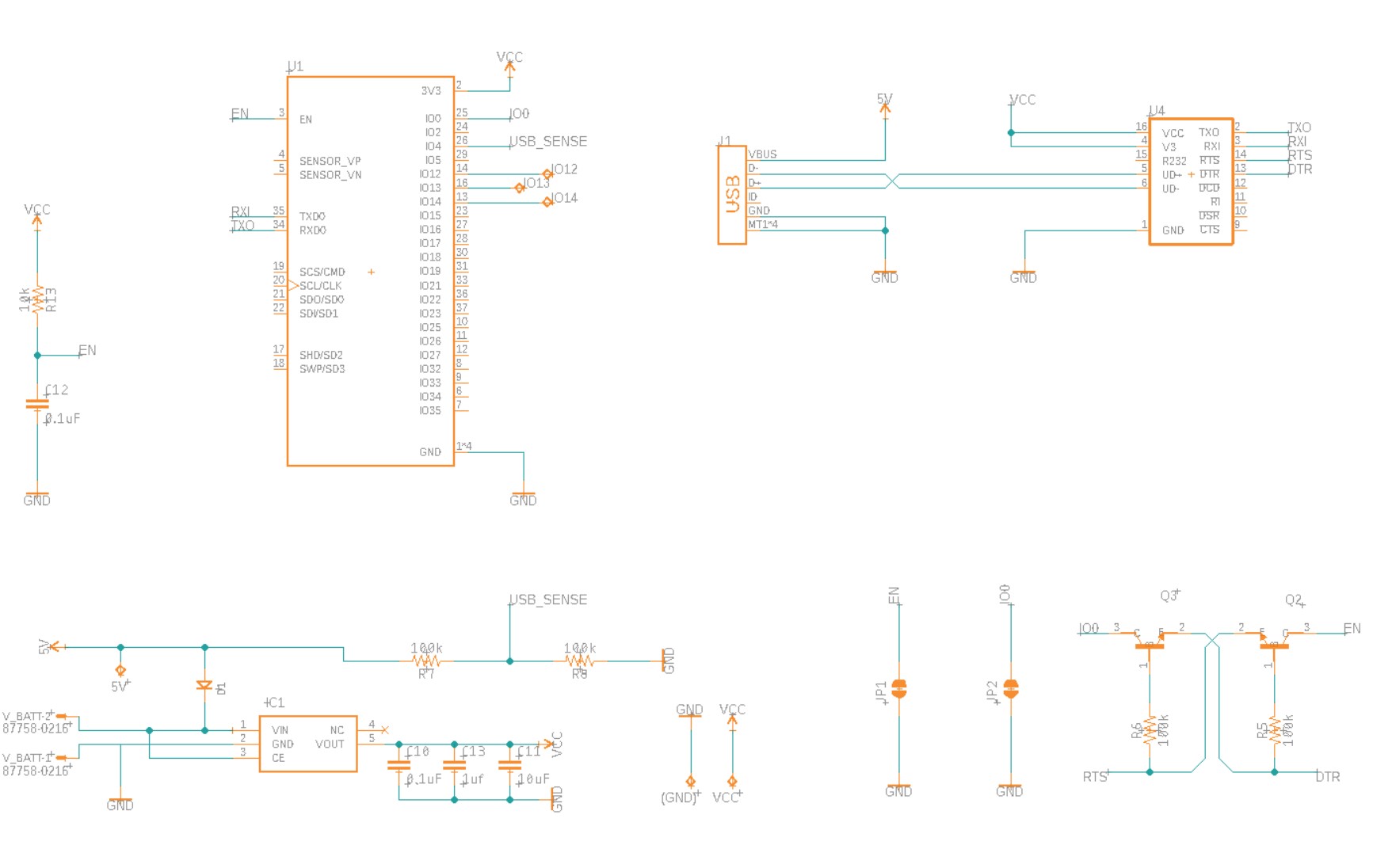
Here is my schematic: PCB Schematic

U1 is the ESP32-WROOM-32 U4 is a CH340C USB to serial chip IC1 is a HT7833 LDO

Lat thing, I've looked at the logic levels on the bootstrapping pins and don't see anything out of the ordinary: GPIO 0: High GPIO 2: Low GPIO 4: Low GPIO 5: High GPIO 12: Low GPIO 15: High

I've been trying to troubleshoot this problem for the past three days and I'm stumped. Any help would be appreciated.

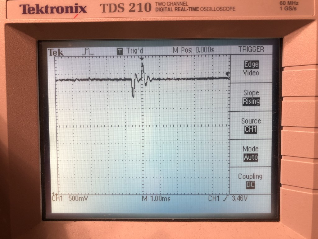
EDIT 1: Here's a picture of the o-scope on VCC. The voltage variance I see is 2.8v on the low end and 3.8v on the high end. enter image description here
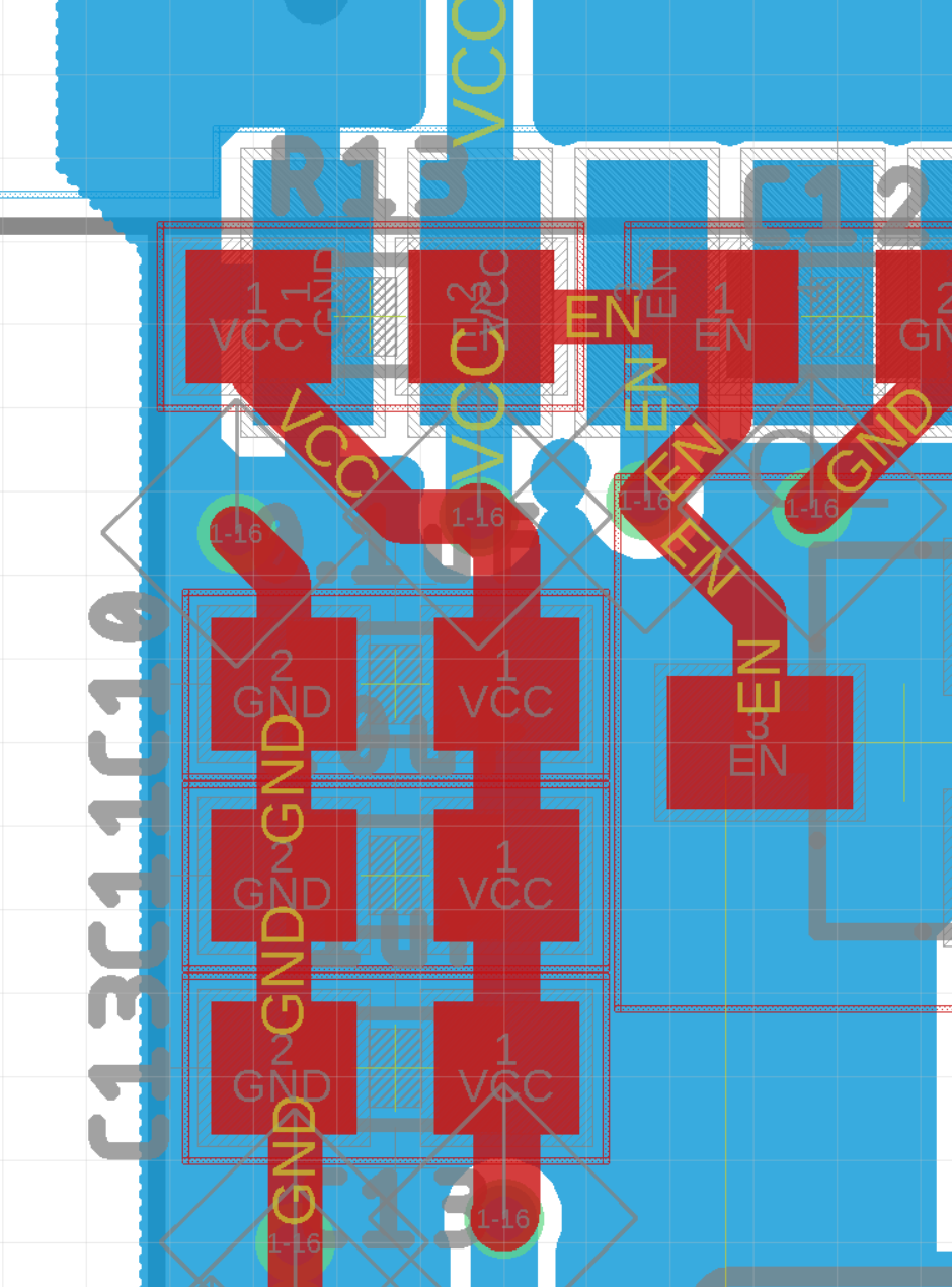
EDIT 2: Capacitor shown on the output of IC1 are positioned extremely closely to U1. See picture: enter image description here
\$\endgroup\$
9
  • \$\begingroup\$ Attach an oscilloscope to the 3.3V at the WROOM32 and see what it does when you access the WiFi. \$\endgroup\$
    – JRE
    Commented Sep 28, 2020 at 7:54
  • \$\begingroup\$ Thanks for the tip @JRE. I just added a photo to my question. It doesn't seem like this voltage spike would cause a problem, no? \$\endgroup\$
    – MikeJWms
    Commented Sep 28, 2020 at 8:36
  • \$\begingroup\$ Decoupling caps ? I can't see if you properly decoupled your IC with decoupling capacitors ? It seems you have some output capacitors on your VCC. But where are they on the layout ? they MUST be extremely close to each VCC pins of every IC. \$\endgroup\$
    – Blup1980
    Commented Sep 28, 2020 at 9:01
  • \$\begingroup\$ @Blup1980 good question. I just edited my original post with a screenshot of that section of the board layout. The capacitors on the output of IC1 are actually positioned right next to the VCC input pin of U1 (esp-32 module). \$\endgroup\$
    – MikeJWms
    Commented Sep 28, 2020 at 9:14
  • 1
    \$\begingroup\$ In my experience, 50-100uF are necessary for stable operation. \$\endgroup\$
    – asdfex
    Commented Sep 28, 2020 at 9:26

1 Answer 1

2
\$\begingroup\$

Thank you for all of the suggestions. I found that adding a 100uF electrolytic capacitor between gnd and VCC solved the problem. I'm also going to test some more powerful LDO's, but until they come in, the cap will work nicely.

\$\endgroup\$
2
  • 1
    \$\begingroup\$ Regardless of the LDO, you'll likely need a good output capacitor. \$\endgroup\$
    – Passerby
    Commented Nov 22, 2020 at 8:07
  • \$\begingroup\$ @Passerby I will keep that in mind, thanks! \$\endgroup\$
    – MikeJWms
    Commented Nov 23, 2020 at 21:33

Your Answer

By clicking “Post Your Answer”, you agree to our terms of service and acknowledge you have read our privacy policy.

Not the answer you're looking for? Browse other questions tagged or ask your own question.