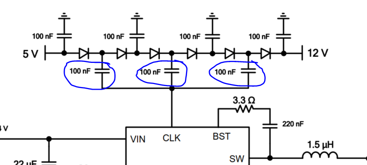
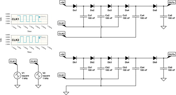
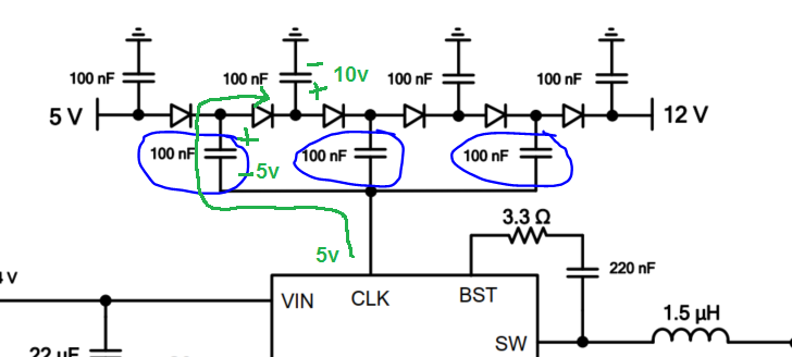
I've simplified and redrawn your two charge pump circuits (or 2 stages of them, at least) in a way that illustrates how they are almost exactly the same:

simulate this circuit – Schematic created using CircuitLab
See how they are equivalent to the two circuits you gave us? The only difference between the two is that in the second example (from the NB680 docs), the second and fourth capacitors are connected to ground, instead of CLK2.
In the top version, because CLK2 is in antiphase with CLK1, each time the capacitors are charged, they "see" twice the potential difference to charge to than the same capacitors in the bottom drawing.
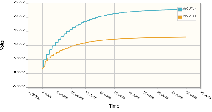
The consequence is that the output voltage of the top circuit is (more or less) twice that of the bottom one. Here are the output voltage curves from the simulation:

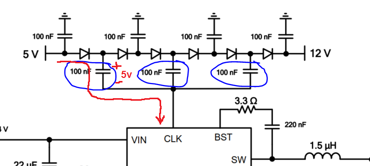
As for your second question, about the factor of 2.5, the only reasons I can think of are that the CLK signal from the NB680 is probably less than 5V, may not even be square, and its frequency of 250kHz doesn't give those capacitors much time to charge between cycles.
 https://www.edn.com/capacitive-voltage-conversion-aka-the-charge-pump/
