I have a device that can be powered by two input supplies, 1) PoE or 2) by a DC input that can accept 5-24V.
Internally, I need a 3.3V rail. I'm using the LM5070 IC reference design (see datasheet) to handle to PoE power conversion, and an LM25117 wide input range synchronous buck controller wired in a very similar way to the application circuit in Fig.29 of its datasheet, to handle the 5-24V DC input conversion to +3.3V.
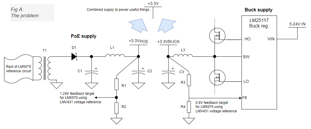
 Fig A. here is a very simplified circuit showing the output sections of these two circuit, where D1 / L1 / C1 / C2 rectify and smooth the PoE output, using the feedback from potential divider R1 / R2 to regulate the output to +3.3V. For the buck regulator, L3 / C3 form the output, with R3 / R4 as the feedback, dividing to 0.8V, to force +3.3V output with appropriate values of R3 / R4.
I would like to combine these input supplies so that if either or both are connected, a single +3.3V rail is available.
So far I've considered relays, ideal diodes, Schottky diode OR'ing etc. to switch between or combine the two +3.3V_POE and +3.3V_BUCK supplies, but no solution seems simple and elegant enough. Note I don't see an obvious way for the presence of input voltage to one supply to be used to disable the other regulator should both input sources be present, which is why I'm looking for a solution to combine outputs in parallel should both input sources be present.
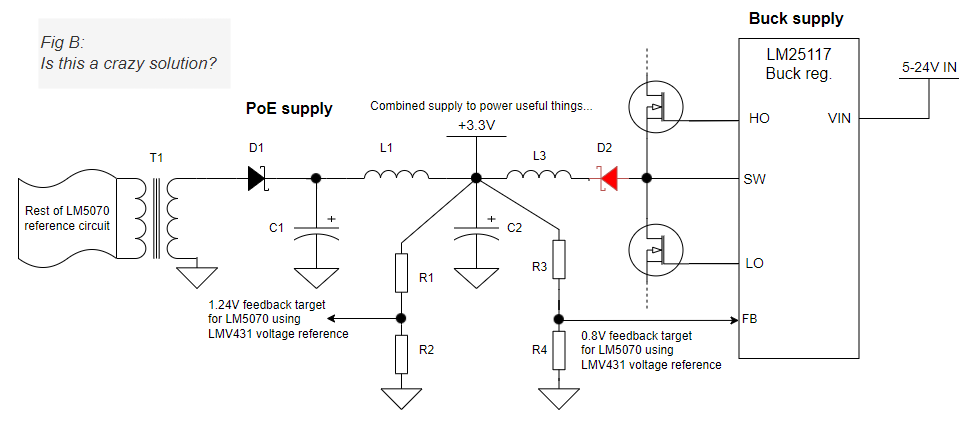
 My question is: can this combining be done simply with the arrangement in Fig.B where the large final output capacitances C2 and C3 are combined to just C2, and diode D2 is added to the buck supply to isolate the LM25117 IC from the +3.3V rail if the 5-24V DC input is not present?
I don't know if the addition of D2 will "upset" the LM25117 as I have not tried this in practice, and there is probably a very fundamental reason that D2 makes no sense - please could somebody explain why this may be if so?
In my understanding, D2 will allow either supply to run with the other powered off, since D1 and D2 mean that one supply can never push current into the other.
When both input sources are present, will both supplies try to create +3.3V with the current shared according to whichever is slightly lower in output impedance and / or higher in output voltage?
Or will D2 "mess up" the feedback loop somehow of the LM25117 as it tries to make R3 / R4 divide the output voltage to the 0.8V reference for this IC? Or is this just a terrible idea for other reasons? Please put me out of my misery!
