1
\$\begingroup\$

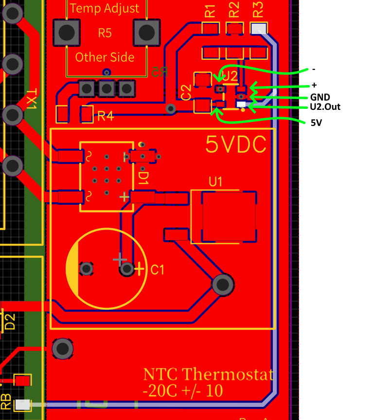
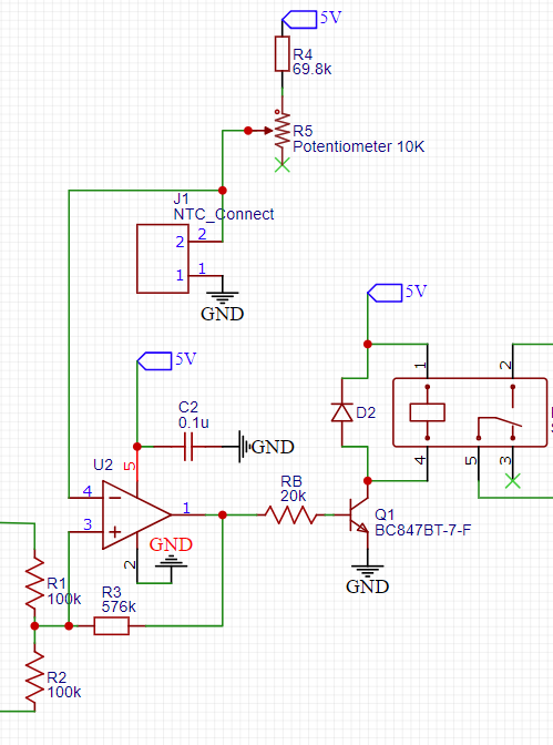
I've put together the circuit from the TI document Comparator with Hysteresis Reference Design using the same reference voltage to the noninverting input (Vth 2.3V - 2.7V). The Inverting input is connected to a voltage divider that depends on a thermistor, but for testing just a potentiometer.

I can confirm that the initial threshold voltage is 2.3V, and that the Power(5V) and GND are correct at pins 5 & 2. When I sweep the inverting input past the threshold voltages, the output never changes from GND.

Ultimately this output is driving the base of an NPN transistor to power a relay, but again, I never get 5V on the output. I actually pulled the first TLV3201 off the board and replaced it, but same issue.

What stupidity have I done?

enter image description here

EDIT - Reference circuit included for clarity.enter image description here
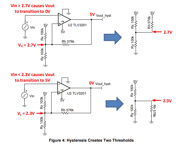
EDIT2 - There is a low impedance path from the U2.1 (comparator output) to GND. Even on a number of blank boards. The board was not designed as such, but I measure 0.1 Ohms between those two pins. See the board image below. The output net is not directly grounded, the only way to GND is supposed to be via R2 + R3 (100K + 576K).

enter image description here

\$\endgroup\$
11
  • \$\begingroup\$ What about pin 3, isn't it floated? \$\endgroup\$ Commented Jan 26, 2022 at 20:58
  • \$\begingroup\$ I chopped the picture so it wasn't too zoomed out, pin 3 is the reference (2.3 - 2.7) that the upper resistor R1 is 5V and the lower R2 is GND \$\endgroup\$
    – pseabury
    Commented Jan 26, 2022 at 21:07
  • \$\begingroup\$ Many comparators have an open-drain or open-collector output. Meaning, the output is a switch that goes to ground. The TLV3201 has push-pull outputs, meaning it can drive high or low. So the chosen comparator should be able to drive up to 100mA. \$\endgroup\$
    – rdtsc
    Commented Jan 26, 2022 at 21:16
  • \$\begingroup\$ The circuit shows the bottom R5 open, did you ground it for the experiment or provide another input voltage at J1? With U2-4 at zero volts what do you measure on all the other pins? \$\endgroup\$ Commented Jan 26, 2022 at 21:24
  • \$\begingroup\$ @KevinWhite That connector is for an NTC thermistor. It and R5 should form a voltage divider, and if it's not connected the input to the comparator will stay at 5V. OP states that the thermistor is not connected, just a potentiometer, which could be the problem if the third terminal of the pot isn't connected to ground. \$\endgroup\$
    – GodJihyo
    Commented Jan 26, 2022 at 21:39

2 Answers 2

1
\$\begingroup\$

Assertions:

  1. There is a false assumption in your BJT calculation for hFE.
    • The hFE applies in the linear region and not the saturated region as a switch. You should not choose a base current, Ib, less than 10% of this expected Ic/hFE min or use the rated Ic/Ib ratio for Vce(sat) which is 20:1 implied from the tables. It is not coincidental, that the B rank hFE= 200 minimum but you must choose a base current of 70 mA/20 = 3.5 mA and thus Rb max= 4.3V/3.5mA = 1.23k max.
  2. There is a short on the board or both IC's you have tested have been damaged as all IC's are 100% tested.
    • Exceeding the do not exceed by any method such as ESD handling damage or DO Not Exceed thresholds exceeded.

    • There should also be an observable voltage change from 0V output as the curves for this CMOS Op Amp indicate an RdsOn at room temp (25'C) of 35 Ohms. Thus you can expect and IR drop from the push-pull CMOS drain outputs.

    • Re-read all the datasheet parameters until understood.

Suggested:

  • check for a short on board.
  • Measure Resistance with power off between gnd. and Output. It must not be low resistance. The DMM current will not exceed the device tolerance of 10 mA for ESD diodes.
\$\endgroup\$
3
  • 1
    \$\begingroup\$ The output pad does measure low impedance to ground. I'm guessing the board has a manufacturing defect as it's not supposed to be that way. I've checked two additional blank boards with the same results. Thanks @Tony I've updated the original question above and added an annotated layout that includes the entire output net. \$\endgroup\$
    – pseabury
    Commented Jan 27, 2022 at 5:11
  • \$\begingroup\$ BTW - can you see any reason why those may be shorted together? I mean, it's a pretty simple board, without exotic features, and fairly large components & traces. Only thing I can think of is that the via in U2.2 somehow has continuity to U2.1 \$\endgroup\$
    – pseabury
    Commented Jan 27, 2022 at 16:11
  • 1
    \$\begingroup\$ Your optics are better than mine. If you can''t see it, you can measure it. Apply several Amps constant current @ < xxx mV and measure uV drop rising with temperature until you fuse to open the short. Move the probe tips around to locate where the resistance is highest. A smart digital Lab supply with DMM probes works well here but you may need a few watts to fuse open (V*I). Others might use brute force methods (Li Ion) or fine distributed Kelvin bridge methods. (Apply current to longest trace and detect jcn. where largest voltage drop occurs) \$\endgroup\$
    – D.A.S.
    Commented Jan 27, 2022 at 16:44
0
\$\begingroup\$

Measure the voltage at pin 4 and make sure it actually goes below the threshold.
If you just have a potentiometer connected between 5V and the input with no path to ground the input voltage will not change enough to trip the comparator.

\$\endgroup\$
1
  • \$\begingroup\$ Yes, U2.4 does measure at both above and below the thresholds as I vary the NTC(pot). U2.3 always stays at 2.3V because the output at U2.1 never goes high. With the U2.4 voltage below 2.3, the output never goes high. \$\endgroup\$
    – pseabury
    Commented Jan 26, 2022 at 22:00

Your Answer

By clicking “Post Your Answer”, you agree to our terms of service and acknowledge you have read our privacy policy.

Not the answer you're looking for? Browse other questions tagged or ask your own question.