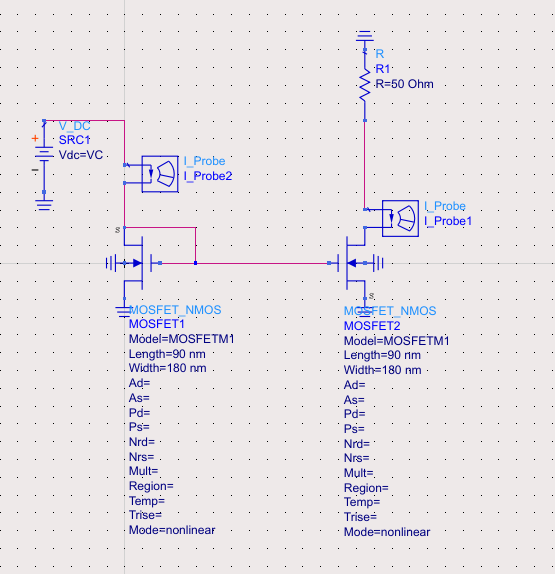
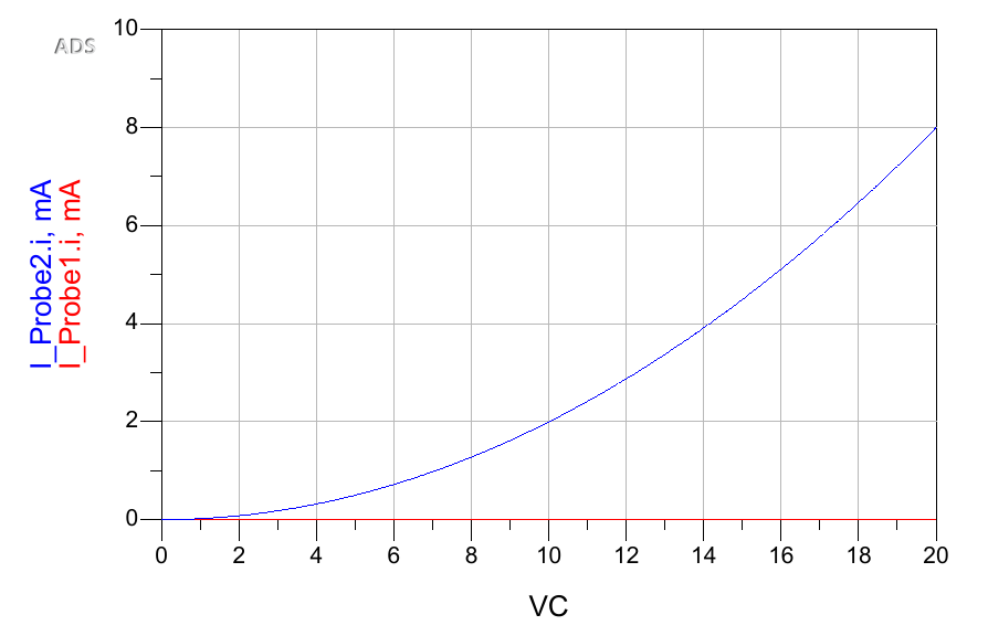
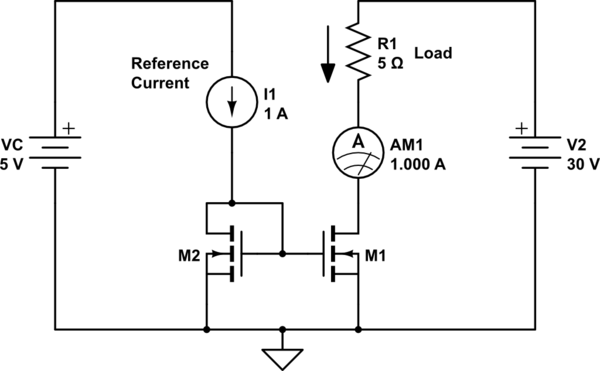
If I understand you correctly, you are trying to establish current down the left (master) side, by controlling the drain voltage of MOSFET1, with the intention of reproducing the same quantity of current down the right (slave) side, via MOSFET2.
Master side
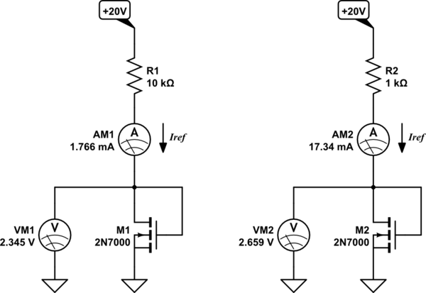
Imposing a voltage directly to the drain of MOSFET1 is not going to give you any control of current there, because that MOSFET must be permitted to decide its own drain voltage. Understand how that MOSFET behaves, with drain connected to gate:

simulate this circuit – Schematic created using CircuitLab
Focus on the voltage between the drain and source, \$V_{DS}\$, as measured by VM1 and VM2. Notice how they are very similar, and for some reason are about 2.5V. On the left, drain current \$I_D = 1.77mA\$, and on the right \$I_D = 17.3mA\$. Why is \$V_{DS} \approx 2.5V\$, and why doesn't it vary much, even for vastly different drain currents?
The connection of drain to gate ensures that gate potential is the same as drain potential, and this has interesting consequences. Imagine that for some reason drain potential rises, bringing the gate with it. In that case, the gate-to-source potential difference \$V_{GS}\$ also increases, and I'm sure you are aware that this is the parameter that decides how "turned on" the MOSFET is. When \$V_{GS}\$ is significantly less than some threshold, the MOSFET is off, significantly greater than that threshold the MOSFET is on, and there's an "active region" around that threshold where the MOSFET is neither on nor off, and the channel resistance (\$R_{DS}\$) varies with \$V_{GS}\$. The threshold I am talking about is of course \$V_{TH}\$ (or \$V_T\$ depending on which datasheet you're reading).
What's going on here is that any rise in drain potential will increase \$V_{GS}\$, causing the MOSFET to conduct better (\$R_{DS}\$ decreases), which acts to lower drain potential back to where it was! In other words, the MOSFET actively fights against a rise in drain voltage.
It also fights against a fall in potential at its drain. when that happens, \$V_{GS}\$ decreases and \$R_{DS}\$ increases, which causes the voltage at the drain to increase, restoring the original state of affairs.
A MOSFET with drain connected to gate like this maintains an equilibrium, where it sits in between on and off states, always on the cusp of saturation, always with \$V_{DS} \approx V_{TH}\$.
Now you are able to see how R1 can be used to control current down that path. In this example, the voltage across R1 is always about \$20V - V_{DS} \approx 17.5V\$, and we may use Ohm's law to find a resistance that will pass whatever current we choose. On the left, drain current is:
$$
\begin{aligned}
I_D &\approx \frac{20 - V_{DS}}{R_1} \\ \\
&\approx \frac{17.5}{10k} \\ \\
&\approx 1.75mA
\end{aligned}
$$
On the right:
$$
\begin{aligned}
I_D &\approx \frac{20 - V_{DS}}{R_2} \\ \\
&\approx \frac{17.5}{1k} \\ \\
&\approx 17.5mA
\end{aligned}
$$
You don't create a reference current by imposing your own voltage at the drain, you must let the drain become whatever voltage the MOSFET chooses. Here we used a resistor to leverage this MOSFET behaviour and pass some desired current.
Slave side
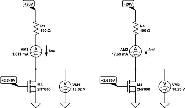
Now I'll create a similar circuit, but this time the drain won't be connected to the gate, and instead I'll explicitly apply a potential, that I choose, at the gate. The voltage I will choose will be the exact same "equilibrium" voltages present at the gates in the circuits above:

simulate this circuit
With no connection from drain to gate, the drain is free to wander up an down in potential. The value of drain resistors R3 and R4 is not important, they represent whatever load you want the mirrored current to flow through.
We rely on precise matching between MOSFETs on the master and slave side, both in characteristics and behaviour, and in temperature, to provide a very similar relationship between \$V_{GS}\$ and \$I_D\$, (which is called transconductance, \$g_m\$). When presented with the same potentials at the gate that the master-side MOSFETS had at theirs, the resulting drain currents \$I_D\$ here are a close match to the drain current on the master side.
Join them together
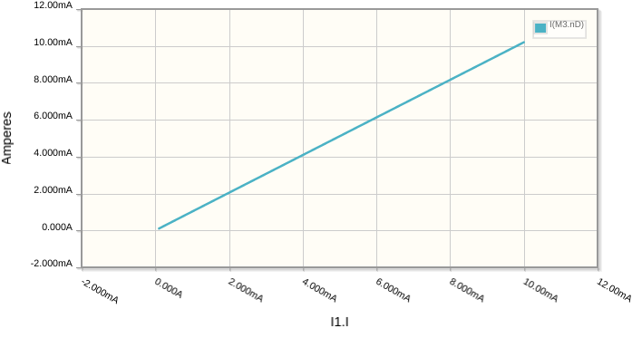
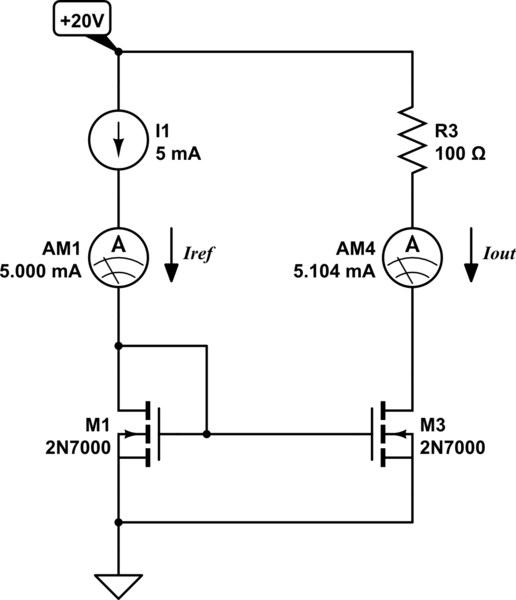
By joining the gates of the two sides together, the gate potentials on both master and slave sides are equal, and consequently \$I_{D\_SLAVE} \approx I_{D\_MASTER}\$. I've done that here, and replaced R1 with a current source to be able to plot a DC sweep:

simulate this circuit
