2
\$\begingroup\$

I've been working with Atmels ATxmega parts a lot recently, and there is one question I still have that I have not been able to find a answer to, even after scouring the datasheets.

Basically, The ADC in the xmega series are somewhat limited by the fact that the \$V_{REF}\$ cannot exceed \$V_{CC}-0.6V\$. This is easily enough accommodated, I am using a 2.048V reference for the ADC with 3.3V rails.

However, I cannot determine if exceeding the ADC \$V_{REF}\$ on the ADC inputs would be actually harmful to the device.

I'm aware exceeding the \$V_{REF}\$ will saturate the ADC, this is fine in this application. However, having to clamp the input to \$V_{REF}\$ would be challenging in my application, as the \$V_{REF}\$ I'm using cannot sink any current, so if I simply used a simple schottky diode to clamp \$V_{in}\$ to \$V_{REF}\$, any excursions of \$V_{in}\$ would simply cause \$V_{REF}\$ to rise as well. I'd really prefer not to have to add a whole additional buffer just to accommodate potential occasional \$V_{in}\$ excursions.

Looking through the datasheet, I'm not really much enlightened:
enter image description here
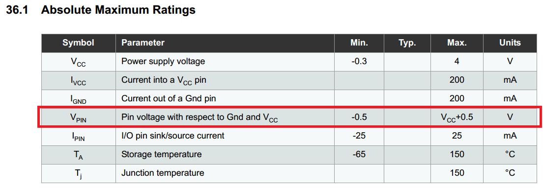
The ADC IO lines are "Pin"s, so I would assume that exceeding the reference, as long as the voltage is kept < \$V_{CC}\$, while the conversion results may be invalid, it won't cause actual damage to the MCU.

On the other hand:
enter image description here
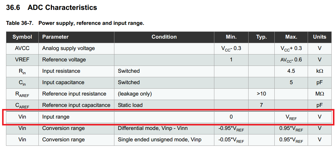
Note that this isn't specified as an "Absolute Maximum" value. I'm not sure if this implies that exceeding these bounds will lead to invalid conversion results, or actual damage.

I've been through both the part-specific datasheet (ATxmega32e5 in this case), and the E series databook, and neither have clarified the issue much for me.

\$\endgroup\$
3
  • \$\begingroup\$ I can't imagine that there would be any problem; the input voltage only relates to the reference voltage via the inputs of a comparator. \$\endgroup\$ Commented Apr 1, 2014 at 6:14
  • \$\begingroup\$ @IgnacioVazquez-Abrams - That's my assumption too, but I'd feel a lot better if I can find it in actual print somewhere, and the fact that I cant makes me uncomfortable. Frankly, the Vcc-0.6V limitation is weird too, so I have no idea what's really going on in the Xmega. \$\endgroup\$ Commented Apr 1, 2014 at 6:16
  • \$\begingroup\$ I couldn't find information about the internal pin protection in the family reference manual, but I did find this thread which suggests that all GPIO pins have the usual clamping diode arrangement. I guess your second highlight from table 36-7 is pointing out the ADC can't read over the Vref. \$\endgroup\$
    – David
    Commented Apr 1, 2014 at 6:37

3 Answers 3

1
\$\begingroup\$

Don't exceed absolute maximum ratings (in fact stay within them as much as you reasonably can). Exceeding Vref isn't a problem providing you don't exceed absolute max ratings. One table is the "don't ever do" table and the other is "don't expect it to function if you do" table.

EDIT - The Vref operational rating of AVcc-0.6V relates more to the DAC outputs on the XMega. DACs share the same voltage reference as the ADCs and because they use the same AVcc power rails, I guess the outputs are restricted to AVcc-0.6V in order to produce non-clipping signals without resorting to extravagant rail-to-rail output amplifiers.

\$\endgroup\$
7
  • \$\begingroup\$ My issue is I haven't found an "absolute maximum" for the ADCs anywhere, and I don't want to assume this is just a plain-old SAR ADC without Atmel at least stating as much somewhere. \$\endgroup\$ Commented Apr 1, 2014 at 7:57
  • \$\begingroup\$ Surely Vpin is the AMR? \$\endgroup\$
    – Andy aka
    Commented Apr 1, 2014 at 7:58
  • \$\begingroup\$ I'd think so, but the Vref AMR is Vpin - 0.6V, so.... maybe? \$\endgroup\$ Commented Apr 1, 2014 at 8:10
  • \$\begingroup\$ I believe that's an operational rating not an absolute rating. \$\endgroup\$
    – Andy aka
    Commented Apr 1, 2014 at 8:14
  • \$\begingroup\$ I don't disagree with anything you're saying, my issue is I can't find anything specific in any of atmel's documentation to confirm it. My gut feeling is that it's probably fine as well, but I don't like to rely on just that. \$\endgroup\$ Commented Apr 1, 2014 at 8:37
1
\$\begingroup\$

Atmel explains this in Application note: AVR1300: Using the Atmel AVR XMEGA ADC.

To quote from 1.4.2:

The voltage on any of the two inputs can be between GND and VREF, but the difference between them must not be larger than VREF/GAIN because this will saturate the ADC and the converted value will only equal the top value of the ADC.

\$\endgroup\$
0
\$\begingroup\$

Im not sure this counts as an answer: I found your question after i extensively searched the net for the same problem! After I could find no answer anywhere (datasheet, application notes, etc.) and I didn't want to screw up one of my current design, I took a ATMEGA168 on a breadboard an run some tests.

@AREF = 2.5V I could ramp up the voltage up to VCC without any damage (I even kept ADC0 for about 30 minutes on VCC). After I played a bit with different voltages I went with the voltage on ADC0 higher than VCC. @About 6V permanent damage occured.

\$\endgroup\$

Your Answer

By clicking “Post Your Answer”, you agree to our terms of service and acknowledge you have read our privacy policy.

Not the answer you're looking for? Browse other questions tagged or ask your own question.