13
\$\begingroup\$

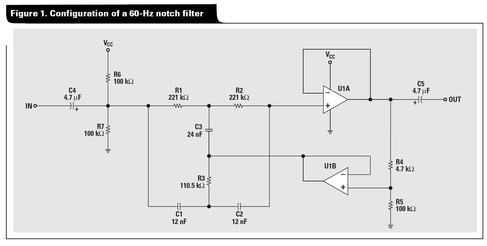
Could anyone give me a hint in analyzing the Twin-T Active Notch Filter? I tried a delta-star transform, followed by nodal analysis, but ended up with conflicting equations. For an example, look at Figure 1 from the Texas Instruments application note "An audio circuit collection, part 2":

enter image description here

In the more general example I am studying, I remove C4/C5 and R6/R7 (and that Vcc) and treat the T passive components as matched conductances as follows:

R1 and R2 become Y1, R3 becomes 2Y1, C1 and C2 become Y2, C3 becomes 2Y2, R4 and R5 generic voltage divider with resistances R1 and R2

\$\endgroup\$
2
  • \$\begingroup\$ This sounds like a question that dsp.stackexchange.com thinks should be on-topic there. What do others think? \$\endgroup\$
    – Kellenjb
    Commented Sep 9, 2011 at 17:02
  • \$\begingroup\$ @Kellenjb - It is on-topic here as well, but might get a better response there. If the OP or the DSP guys want it migrated, we can do that - it certainly could deal with a bit more attention. Alternatively, draw up a schematic and upload the image to bump this to the front page where it should get more attention....not sure how it got missed the first time around. \$\endgroup\$ Commented Oct 8, 2011 at 21:09

2 Answers 2

7
\$\begingroup\$

The Delta-Star transform can be used to analyze the Twin-T network using the following procedure:

  1. The two T networks can be converted into twin Delta networks in parallel: enter image description here
  2. Condense these two Delta networks into a single Delta network
  3. Convert the resulting Delta network back into a T network.

  4. To see the notch behavior of the passive twin T, assume node 2 is tied to ground, and treat the Delta network you got in step 3 as a voltage divider.

    You'll find a transfer function of $$H(s) =\frac{s^2 + {\omega_0}^2}{s^2 + 4s\omega_0 + {\omega_0}^2}$$.

  5. To see the effect of bootstrapping, assume that node 2 is held at a voltage αVout, where α is some scaling factor between 0 and 1. The T-network still acts as a voltage divider, dividing between Vin and αVout. To find the behavior of the system, we need to solve the equation $$v_\textrm{out} = \alpha \cdot v_\textrm{out} + H(s) ( v_\textrm{in} - \alpha\cdot v_\textrm{out} )$$, where $$H(s)=Z_2/(Z_1 + Z_2)$$ is the transfer function without feedback. Doing this, we find a new transfer function: $$G(s) = \frac{1}{(1-\alpha)\frac{1}{H(s)} + \alpha}$$. Note that for \$\alpha=0\$ (no feedback), we have \$G(s)=H(s)\$, as expected. For \$\alpha=1\$, the system becomes unstable. Plotting this function for values of alpha between 0 and 1, we find a huge increase in the Q of the notch.

The resulting transfer function is: $$G(s) =\frac{s^2 + {\omega_0}^2}{s^2 + 4s\omega_0(\alpha - 1) + {\omega_0}^2}$$.

Here's what the frequency response looks like, as the feedback gain \$\alpha\$ is changed:
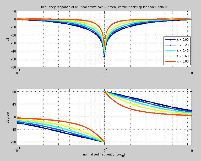
Frequency response of an ideal twin T notch The algebra of the various transforms is a bit tedious. I used Mathematica to do it:

(* Define the delta-star and star-delta transforms *)

deltaToStar[{z1_,z2_,z3_}]:={z2 z3, z1 z3, z1 z2}/(z1+z2+z3)
starToDelta[z_]:=1/deltaToStar[1/z]

(* Check the definition *)
deltaToStar[{Ra,Rb,Rc}]

(* Make sure these transforms are inverses of each other *)
starToDelta[deltaToStar[{z1,z2,z3}]]=={z1,z2,z3}//FullSimplify
deltaToStar[starToDelta[{z1,z2,z3}]]=={z1,z2,z3}//FullSimplify

(* Define impedance of a resistor and a capacitor *)
res[R_]:=R
cap[C_]:=1/(s C)

(* Convert the twin T's to twin Delta's *) 
starToDelta[{res[R], cap[2C], res[R]}]//FullSimplify
starToDelta[{cap[C], res[R/2], cap[C]}]//FullSimplify

(* Combine in parallel *)
1/(1/% + 1/%%)//FullSimplify

(* Convert back to a T network *)
deltaToStar[%]//FullSimplify

starToVoltageDivider[z_]:=z[[2]]/(z[[1]]+z[[2]])
starToVoltageDivider[%%]//FullSimplify

% /. {s-> I ω, R ->  1/(ω0 C)} // FullSimplify
\$\endgroup\$
2
\$\begingroup\$

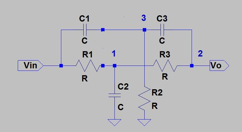
Here's one way to go about it - the notch filter with feedback is a little more complicated so for the time being I'll just outline how to do the general form of the twin-T notch filter:

enter image description here

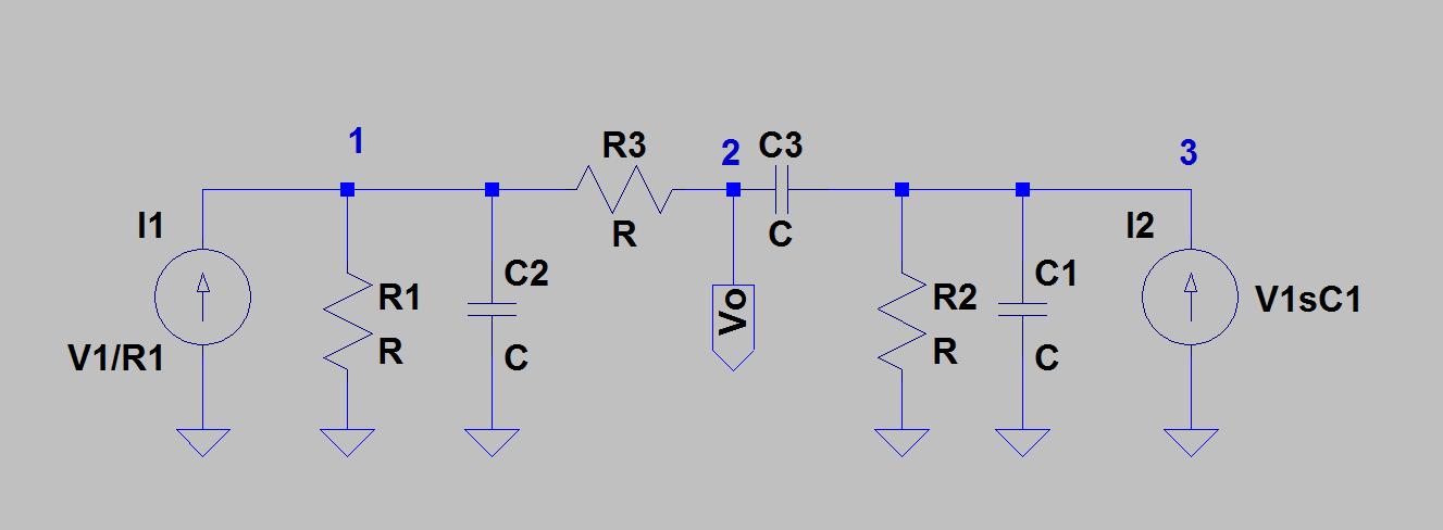
To solve the circuit using nodal analysis what to do is convert the voltage source Vin to its equivalent Norton source - its a little tricky though because you have to convert Vin into two Norton sources to account for R1 and C1 and then rearrange the circuit to compensate. Like this:

current source version

Points 1, 2, and 3 are shown in their new positions on the equivalent circuit. You should then be able to write down KCL equations by inspection and create a 3 by 3 augmented matrix in the unknowns V1, V2, and V3. You can then solve for V2/Vo in terms of Vin by using Cramer's rule.

The feedback circuit as shown in the TI datasheet shouldn't be that much more complicated, since the output is buffered by U1A and U1B then you could create a similar current source equivalent circuit; instead of R2 and C2 in my first diagram going to ground they would be connected to a voltage source with a value of \$Vo*\alpha\$, where alpha is the voltage division ratio.

Edit: corrected first diagram

\$\endgroup\$

Your Answer

By clicking “Post Your Answer”, you agree to our terms of service and acknowledge you have read our privacy policy.

Not the answer you're looking for? Browse other questions tagged or ask your own question.