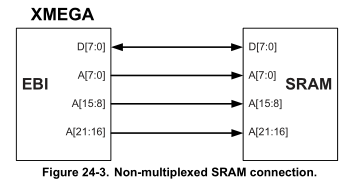
A memory chip isn't generally going to care if all the address wires switch at the same time. The most that would typically be required would be that all address wires be set to their proper levels before an access is initiated, and that they remain at their proper levels for some amount of time after the access is complete. In many cases, the requirements for read accesses are even looser than that: if the address on the bus changes during a read, many devices will effectively automatically initiate an access with the new address, and prevent valid data within some period of time of the last change to the address bus.
Since using one I/O pin for each address line would gobble up a lot of I/O, it may be helpful to add one or more latches or registers. For example, one could address up to 16MB of memory while using nine pins for addressing. Connect eight of them to address bits 0-7 as well as the inputs of a 74HC373 and a 74HC374. Feed the remaining pin to the load-enable and clock signals of those chips. Connect the outputs of the 74HC373 to address bits 8-15, and those of the 74HC374 to address bits 16-23.
To access a particular byte, start with "Clock/LE" low and do the following in order:
- Output bits 16-23 of the desired address.
- Drive "Clock/LE" high.
- Output bits 8-15 of the desired address.
- Drive "Clock/LE" low.
- Outputs bits 0-7 of the desired address
- Hit whatever other pins are necessary to trigger the desired access.
Additional accesses within a 256-byte range may be accomplished by repeating steps 5-6 (omitting steps 1-4).
A variety of arrangements are possible depending upon speed requirements and the number of I/O pins you have available.

