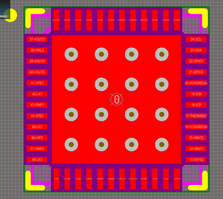
I used the component wizard in Altium to automatically create a footprint but it decided to overlap the solder mask expansion with neighboring pads. Is this ok or should I change it such that there is a gap between each pad.
-
2\$\begingroup\$ What's the pin pitch of your part. Altium's defaults won't leave a solder mask sliver between pins on 0.65-mm-pitch QFN parts, but the shop I work with can deal with a small enough expansion and thin enough sliver to allow one (0.075 mm expansion and 0.075 mm sliver, IIRC). Point is, sometimes you have to find out what your shop's capabilities are, not just use Altium's defaults. \$\endgroup\$– The PhotonCommented Oct 4, 2016 at 4:21
3 Answers
The overlap is not a problem as far as having the PCB green-board made. There will just be no soldermask everywhere you see the purple.
This could be a problem when you have the boards populated, because solder bridging is more likely.
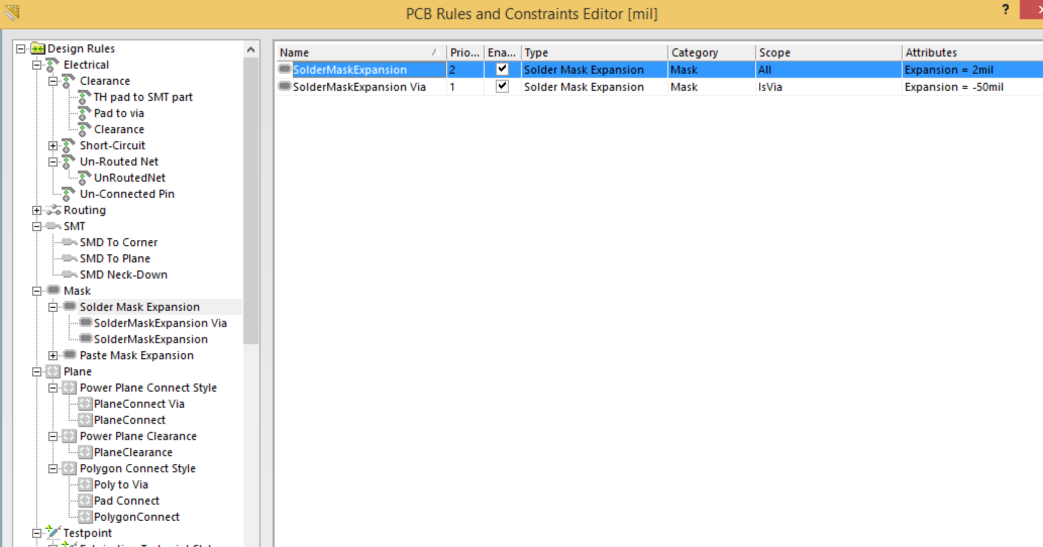
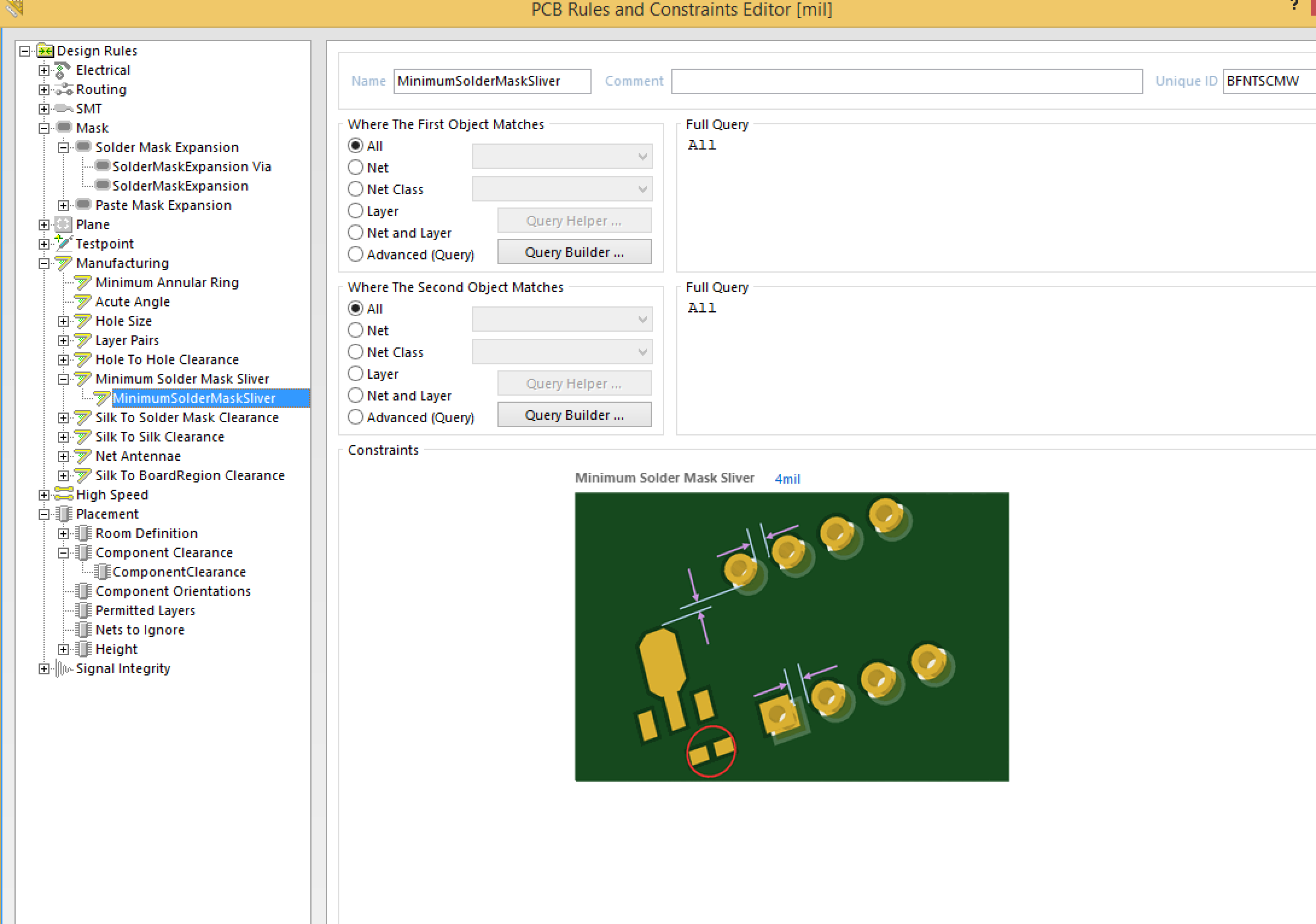
The real answer here is that you should work with your board house and determine what the solder mask expansion and minimum sliver size should be (the smallest sliver between pads).
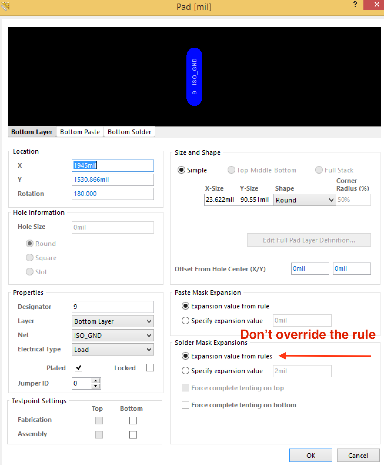
Also, check your part to make sure the rule isn't overridden:
It's fine, and when the pads are closer together than the manufacturing process can handle (the sliver between pads disappears or becomes too narrow to meet capabilities) there is no other way. Especially for 0.4mm pitch and similar really fine pitches.
It probably makes shorts between pins a bit more likely, so check capabilities of your board houses and see if it is feasible to edit the footprint.
IPC actually recommends a 1:1 Soldermask to Pad Size ratio, and just letting the Manufacturer decide the Soldermask Swell required.


