1
\$\begingroup\$

I have two questions. First paragraph is background, second is questions.

Background:

I have a photodiode amplifier (low capacitance APD + fast transimpedance amplifier) that has a nice response with small amplitude light pulses. It has good phase margin and there is no overshoot.

When I increase the amplitude of the incoming light pulse, the amplifier output will get close to or hit the rail, and I get overshoot and ringing.

Questions:

  1. How do I analyze amplifier phase margin with a large signal response that may saturate the amplifier?

  2. How do overdrive recovery circuits work? I can't find any reference to overdrive recovery in my Gray & Meyer book. Where can I learn more about overdrive recovery?

Thanks

\$\endgroup\$
9
  • \$\begingroup\$ Read the data sheet for (1) and for (2) use zeners and negative feedback to prevent output saturation. With some high values of feedback resistor this may not be appropriate. \$\endgroup\$
    – Andy aka
    Commented May 30, 2017 at 17:58
  • \$\begingroup\$ hi david, i currently facing the same problem as you discussed, i thought the ringing is due to capacitive load of probe, but its not, i observe it only in saturation, how did you avoid this ?, kindly provide the observation details \$\endgroup\$
    – kakeh
    Commented Sep 20, 2017 at 7:41
  • \$\begingroup\$ @kakeh my solution was similar to analogsystemsrf circuit using automatic gain control. A diode in the feedback loop switches in a resistor in parallel with a capacitor with the same time constant as the normal feedback but with much less resistance and more capacitance. This resistance * your largest input current needs to be less than the maximum output voltage of your op amp. This way the op amp always stays in its linear region. \$\endgroup\$
    – DavidG25
    Commented Sep 20, 2017 at 14:00
  • \$\begingroup\$ my diode is AD1500 from first sensor, peak current is 0.25mA, my opamp is 2.5V rail with 10K and 1.6p combination in feedback, but when i laze a 40ns (i understand my ckt BW is 10MHz)pulse at the photo diode i dont see saturation instead i see a expansion of pulse to 400ns why so ? are you trying to say me to keep the saturation current opamp lower than diode peak current. is pulse expanding due to BW constraint ? \$\endgroup\$
    – kakeh
    Commented Sep 21, 2017 at 3:08
  • \$\begingroup\$ my opamp LT6269 can handle even up to 10ns, so i have replaced 10k with 1k to make sure opamp never saturates, as saturation current will be 2.5mA where as diode peak current is 0.25mA, but then i have seen the effect you explained, is ringing due to opamp saturation or APD saturation ? there is no way APD can provide such high current of 2.5mA as the peak itself is 0.25mA. \$\endgroup\$
    – kakeh
    Commented Sep 21, 2017 at 3:40

2 Answers 2

1
\$\begingroup\$

1) Predicting overload recovery from small-signal behavior is a lost cause. It depends entirely on things like the input transistor characteristics and the thermal characteristics of the die.

2) Overdrive protection circuits work (typically) by shunting overdrive current away from the input stage. As a result, the input does saturate, but just barely. A typical example would be providing back-to-back diodes across the input (at the expense of increased input capacitance and slightly increased input current).

\$\endgroup\$
4
  • \$\begingroup\$ Where can I learn more about this? Could you recommend a book? I don't think my Analysis and Design of Analog ICs covers this. \$\endgroup\$
    – DavidG25
    Commented May 30, 2017 at 21:34
  • \$\begingroup\$ Also, wouldn't back to back diodes let the inverting input get a diode drop above or below the non-inverting input before current started to get shunted away? At that point the amplifier would be saturated. How can I shunt current away from the input earlier? \$\endgroup\$
    – DavidG25
    Commented May 30, 2017 at 23:19
  • \$\begingroup\$ @DavidG25 - Yes. But that's better than no limit at all. And I'm not aware of any book on the subject. \$\endgroup\$ Commented May 30, 2017 at 23:48
  • \$\begingroup\$ @WhatRoughBeast i am facing a similar problem, i tried to explain it here kindly throw some comments electronics.stackexchange.com/questions/331423/… \$\endgroup\$
    – kakeh
    Commented Oct 4, 2017 at 3:04
1
\$\begingroup\$

You have slew-rate limiting at the large signal outputs, which is a time-delay.

Can you add a tiny capacitance across Rfb, value only 10% of what works at small amplitudes but providing the necessary "look ahead" for large inputs?

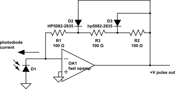
Or simulate this variable-gain TIA

schematic

simulate this circuit – Schematic created using CircuitLab

\$\endgroup\$
2
  • \$\begingroup\$ This kind of reminds me of the gain limiting circuit I've used on wein-bridge oscillators to get less distortion. I'm not sure I can decrease my feedback resistance since I am using a CFB op amp that is tuned as fast as possible without overshoot. Would it be correct to think that adding small signal phase margin may compensate for the open loop phase taking a hit at large signal amplitudes due to slew-rate limiting time delay? I have a little bit of room to slow down my amplifier. \$\endgroup\$
    – DavidG25
    Commented May 31, 2017 at 18:43
  • \$\begingroup\$ i am facing a similar problem , kindly throw some light electronics.stackexchange.com/questions/331423/… \$\endgroup\$
    – kakeh
    Commented Oct 4, 2017 at 3:05

Your Answer

By clicking “Post Your Answer”, you agree to our terms of service and acknowledge you have read our privacy policy.

Not the answer you're looking for? Browse other questions tagged or ask your own question.