6
\$\begingroup\$

Below on the left side of the illustration there is a point-contact transistor which is the first transistor invented in 1947:

enter image description here

It seems the symbol of BJT actually comes from this point-contact transistor even though they operate very different way.

But what is the purpose of using a "spring" for establishing contacts?

In this source it is written:

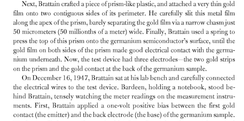
The whole triangle was then held over a crystal of germanium on a spring, so that the contacts lightly touched the surface.

Is that the reason for using the spring? To ensure a weak touch to the germanium surface? But if so, why is a weak/lightly touch is needed?

Edit:

Another source from page 201 of the book called "Conquering the Electron":

enter image description here

\$\endgroup\$
1
  • \$\begingroup\$ looks like a female emitter (lol) , maybe they thought base resistance must be higher for more better current gain and not disturb charge flow between CE \$\endgroup\$
    – D.A.S.
    Commented Mar 30, 2018 at 16:13

3 Answers 3

9
\$\begingroup\$

You need enough force to maintain contact, but not so much that you crack the Ge crystal.

If you just directly connected the contact to the structure shown holding the spring, with no flexibility, it would be very easily to apply excess pressure and damage the crystal.

\$\endgroup\$
19
  • \$\begingroup\$ Yet Germanium has a shear modulus (GPa) slightly greater or same as Titanium and same Young's modulus for elasticity. \$\endgroup\$
    – D.A.S.
    Commented Mar 30, 2018 at 16:27
  • \$\begingroup\$ So being extremely rigid and probably if used as very thin slice makes it too sensitive for applied force? \$\endgroup\$
    – user16307
    Commented Mar 30, 2018 at 16:29
  • 3
    \$\begingroup\$ @TonyStewart.EEsince'75, 1. Silicon has even higher shear modulus and is still easily cracked when in millimeter-thick crystals. 2. Shear modulus doesn't tell you anything about shear strength. \$\endgroup\$
    – The Photon
    Commented Mar 30, 2018 at 16:39
  • 1
    \$\begingroup\$ @TonyStewart.EEsince'75 That triangle is the plastic(if you mean huge for that), I think he is talking about the germanium at the bottom. \$\endgroup\$
    – user16307
    Commented Mar 30, 2018 at 16:51
  • 1
    \$\begingroup\$ As I understand the cat's whisker method of maintaining a junction, too much pressure pushes the assembly into full conduction. I'm having trouble finding a reference that doesn't feel anecdotal, though. Was this not the case? \$\endgroup\$
    – user39962
    Commented Mar 30, 2018 at 23:24
13
\$\begingroup\$

Here are some experimental results I have obtained with a galena detector.

Preamble

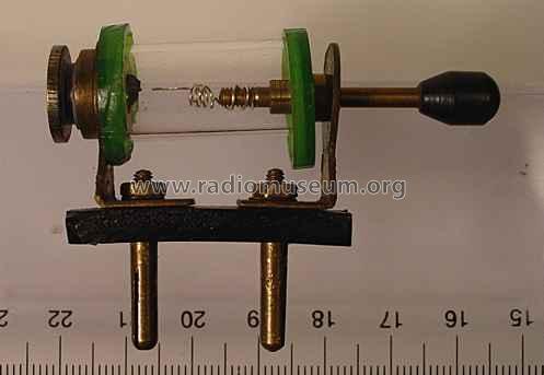
Galena detectors were the predecessor of diodes. It was composed of a galene cristal and a needle of copper in contact with it. So far I know galena detectors always have a compression spring.

Here is such a detector similar to the one I have tested. One can see the spring.

enter image description here

The tests were done with a curve tracer.

Results

To obtain a detector effect, the pressure must not be too much nor too light.

Thanks to the spring the operator is able to master this pressure. For this reason, the spring is clearly essential

The best results (ie non-linearity) are obtained when one first apply a little bit to much pressure then release progressively the pressure until a good non-linear curve appears on the screen of the curve tracer.

I don't have the theory behing this. Maybe the first pressure flattens or cleans the surface (oxyded ?), but I seem to recall that when one apply once again more pressure after having obtained a good result, things are worse.

So the modelisation of this kind of problem seems to be complicated. There are some effects with memory that can improve the results.

\$\endgroup\$
3
  • 1
    \$\begingroup\$ For those of us that grew up in the 50s, the "crystal radio" was a "thing" -- just about anyone with a technical bent would build one (often from a kit). The "crystal" took many forms, often (in the "foxhole radio") being the oxidized coating on a razor blade. Pressure for the point contact was typically supplied by a bent piece of modestly stiff wire. The point contact itself was often a piece of carbon-clay pencil "lead". \$\endgroup\$
    – Hot Licks
    Commented Mar 30, 2018 at 23:57
  • \$\begingroup\$ I don’t know if it applies to the (manmade?) crystal in the transistor case, but part of the reason for the adjustable whisker contact on galena diodes was so that you could make contact with just on crystal face. That got the best rectification. \$\endgroup\$ Commented Mar 30, 2018 at 23:59
  • \$\begingroup\$ related \$\endgroup\$
    – andre314
    Commented Nov 29, 2018 at 18:04
0
\$\begingroup\$

The junction had to be formed by pulsing a current through it. It needed a light pressure or the junction would be to deep. In forming a tunnel diode the pressure is moderate and the well is more profound. Anyway the two wells can not touch or the transistor is destroyed. The playoff is two wells very close together but not touching. You might find this interesting: http://radio.radiotrician.org/2018/04/the-mystery-of-how-point-contact.html

\$\endgroup\$

Your Answer

By clicking “Post Your Answer”, you agree to our terms of service and acknowledge you have read our privacy policy.

Not the answer you're looking for? Browse other questions tagged or ask your own question.