1
\$\begingroup\$

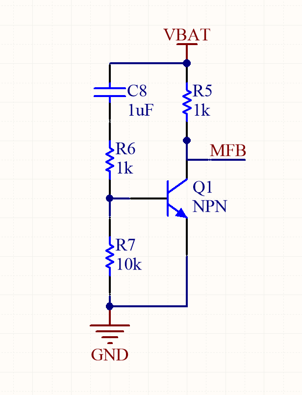
I need some help to figure out what this NPN transistor circuit do, how it works and why it's needed in order to make the CSR64215 bluetooth chip work. Here's the schematic:

MFB circuit

And here's what MFB stands for in CSR64215 chip (took it from the datasheet): VREG_EN/MFB pin explanation


I'm asking all these questions because I'm about to use this bluetooth chip in my car and the problem I'm facing right now is that when I'm cranking the engine it turns off and back on quickly, but after that it unables to connect to my phone automatically and it's very frustrating as you have to do it manually after all. So basically I'm looking for a fix for this issue.

\$\endgroup\$

3 Answers 3

4
\$\begingroup\$

The circuit, even with the diode is a piece of junk. The 11ms time constant without the diode was pretty short.

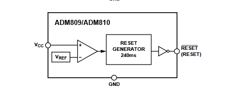
Either regulate the supply so it doesn't drop during cranking or use a proper reset chip that provides a timed reset pulse of appropriate duration for a complete reset for any brownout of the supply.

enter image description here

\$\endgroup\$
3
  • \$\begingroup\$ I've tried to use ADM809 and it works much better than before and most of time my phone connects to the bluetooth module automatically, but still sometimes it fails to do so.. I guess 240ms reset active timeout is a little bit to low. How I can increase this timeout? 1s would be ideal.. \$\endgroup\$ Commented Sep 1, 2018 at 19:30
  • \$\begingroup\$ That model is not adjustable. If you go to a distie like digikey.com and search "PMIC - Supervisors". you'll find plenty of options Eg. NCP302/3 series or TPS3808. \$\endgroup\$ Commented Sep 1, 2018 at 23:56
  • \$\begingroup\$ Many thanks! This is exactly what I was looking for. I hope this will work... \$\endgroup\$ Commented Sep 3, 2018 at 9:00
7
\$\begingroup\$

The only reference to "MFB" in the CSR64215 datasheet is the VREGENABLE signal on pin 40. In the datasheet there's a pushbutton switch to connecting VREGENABLE to Vbat.

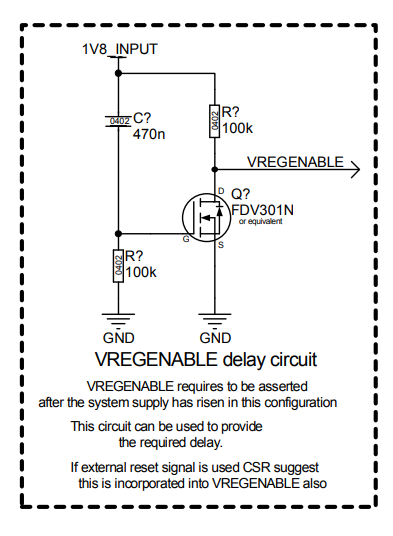
The circuit you show is similar to the VREGENABLE delay circuit on page 69 of the datasheet:

enter image description here

How does this circuit work?

When the supply voltage (1V8_INPUT, VBAT in your circuit) becomes active the capacitor will charge. This causes a current to flow through the resistor in series with the capacitor (R7 in your schematic). This then activates the NMOS or NPN which will then pull down the output VREGENABLE (MFB in your circuit).

After some time (about RC = 10 kohm * 1 uF = 10 ms, this is a ballpark figure, not very accurate!), a couple of milli seconds, the capacitor is charged and the charging current becomes zero. Then there is no voltage to activate the NMOS / NPN anymore so it opens and the VREGENABLE output (MFB in your circuit) becomes equal to the supply voltage (1V8_INPUT, VBAT in your circuit).

So your circuit makes MFB high after some delay, when VBAT is switched on.

\$\endgroup\$
3
  • 1
    \$\begingroup\$ Note the bug in this (and many similar) circuits : if you switch off and back on quickly enough, the capacitor remains charged and the requisite delay is absent on the second power cycle, possibly causing mis-operation. The usual fix is a diode to discharge the capacitor, by conducting if (in this example) C (lower terminal) goes below 0V. \$\endgroup\$
    – user16324
    Commented Jul 5, 2018 at 9:37
  • 1
    \$\begingroup\$ @BrianDrummond it's like you're reading my mind. This is exactly the reason why I'm asking all these questions - I want to fix this as I'm about to use this chip in my car and the problem I'm facing right now is that when I'm cranking the engine it turns off and back on quickly, but after that it unables to connect to my phone automatically and it's very frustrating as you have to do it manually after all. Where I should put the diode in my provided schematic so it works as you described? Thank you! \$\endgroup\$ Commented Jul 5, 2018 at 10:01
  • 1
    \$\begingroup\$ Place that diode across the charging resistor but such that it does not conduct in normal operation (when the supply is present). So Anode to ground, Cathode to capacitor bottom - side (same node as the base of the NPN). Oh, it's drawn in Brian's answer :-) \$\endgroup\$ Commented Jul 5, 2018 at 10:28
5
\$\begingroup\$

To expand on my comment and answer the additional question:

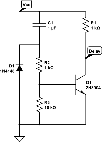
Note the bug in this (and many similar) circuits : if you switch off and back on quickly enough, the capacitor remains charged and the requisite delay is absent on the second power cycle, possibly causing mis-operation. The usual fix is a diode to discharge the capacitor, by conducting if (in this example) C (lower terminal) goes below 0V.

Schematic with bug fix.

schematic

simulate this circuit – Schematic created using CircuitLab

In normal operation D1 does nothing. But when VCC falls to 0, the charge stored on the capacitor pulls D1 cathode negative (below 0V). D1 then conducts, discharging the capacitor much faster than would otherwise happen, to ensure the Delay occurs as expected when power is restored.

\$\endgroup\$
3
  • 2
    \$\begingroup\$ You're amazing guys! Thank you both Brian and Bimpelrekkie for comprehensive answers with all the details! Now it's time to try this out in my application. \$\endgroup\$ Commented Jul 5, 2018 at 10:37
  • 1
    \$\begingroup\$ Diode is a good improvement suggestion. \$\endgroup\$
    – User323693
    Commented Jul 5, 2018 at 17:41
  • \$\begingroup\$ @Brian Drummond I've tried to use a diode like in example you provided, but it doesn't seems to work for me :( Another solution would be probably to use ADM809 instead? \$\endgroup\$ Commented Jul 20, 2018 at 10:05

Your Answer

By clicking “Post Your Answer”, you agree to our terms of service and acknowledge you have read our privacy policy.

Not the answer you're looking for? Browse other questions tagged or ask your own question.